

Fairchild Semiconductor FAN8001BD Datasheet
©2000 Fairchild Semiconductor International
www.fairchildsemi.com
Rev. 1.0.1
February. 2000.
1
Features
• 1 phase, full-wave, linear DC motor driver
• Built-in TSD (Thermal shutdown) circuit
• Built-in 5V regulator (With an external PNP TR)
• Built-in mute circuit
• Built-in loading motor speed control circuit
• Wide operating su pply voltage range: 6V~13.2V
Description
The FAN8001D is a monolithic integrated circuit, suitable
for 5-ch motor driver which drives focus actuator, tracking
actuator, sled motor , spindle motor and loading motor of CD
system.
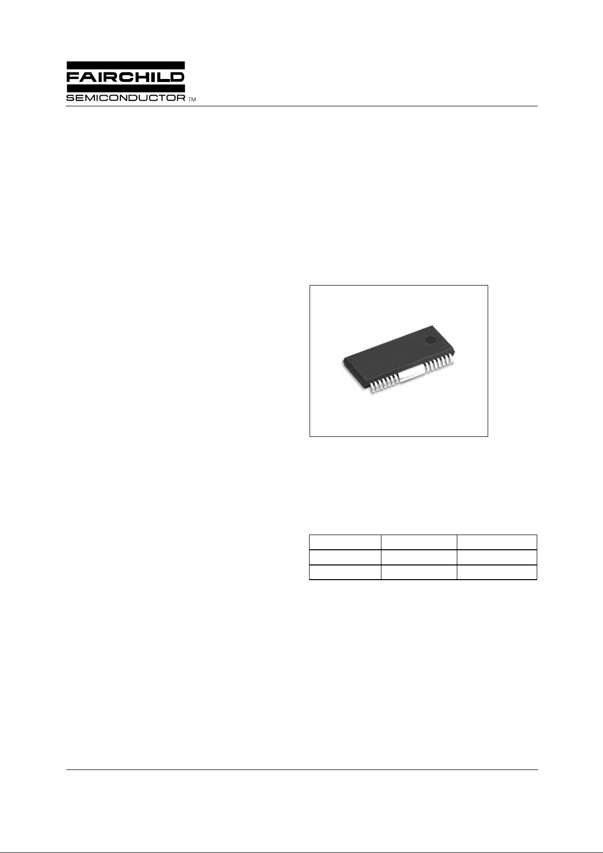
28-SSOPH-375
Target Applications
• Compact dis k player (CDP)
• Video compact disk player (VCD)
• Automotive compact disk player (CDP)
• Other compact disk media
Ordering Information
Device Package Operating Temp.
FAN8001BD 28-SSOPH-375 −25°C ~ +75°C
FAN8001BDTF 28-SSOPH-375 −25°C ~ +75°C
FAN8001D
5-Channel Motor Driver
FAN8001D
2
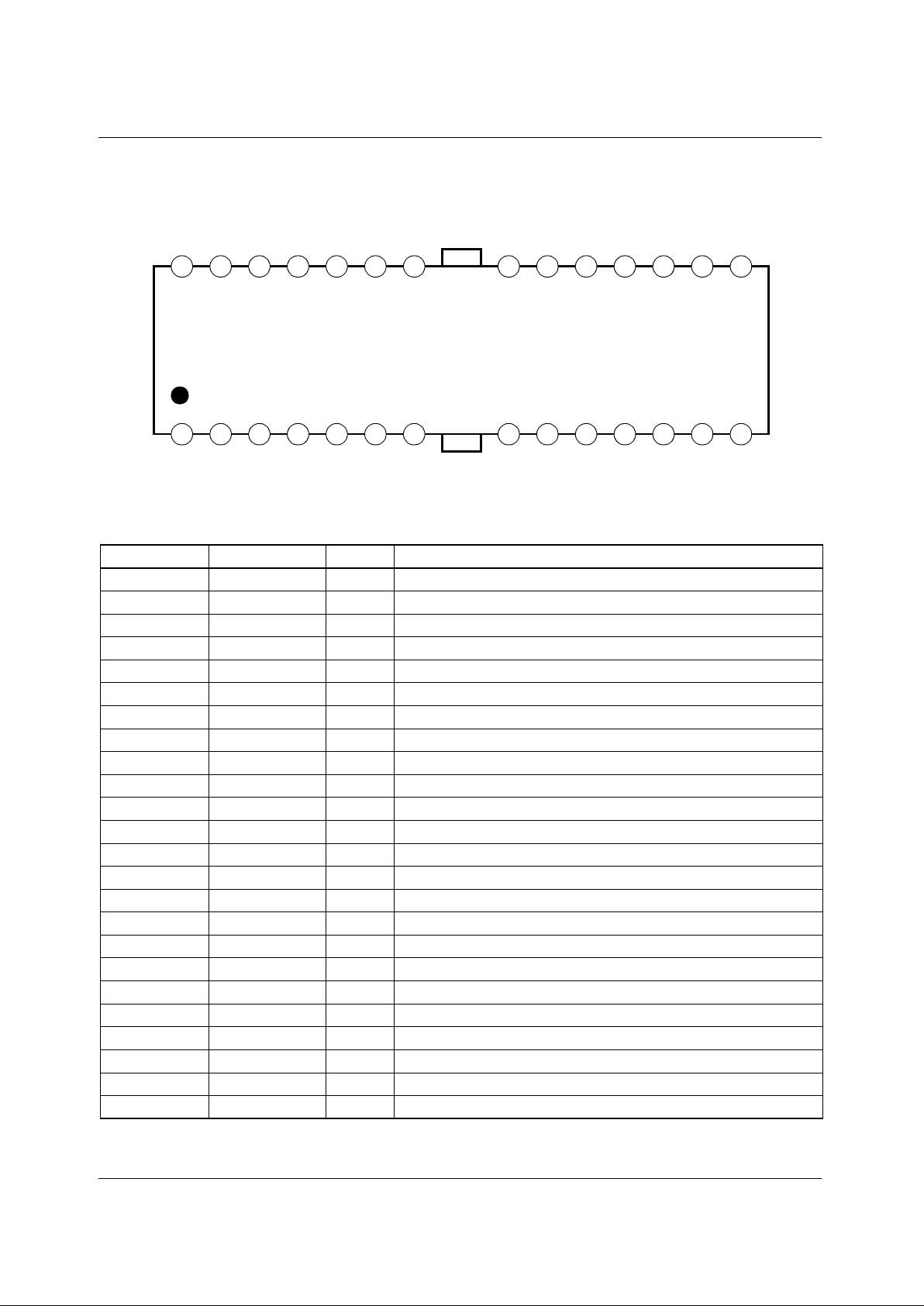
Pin Assignments
Pin Definitions
Pin Number Pin Name I/O Pin Function Description
1 DO1.1 O Focus output 1 (−)
2 DO1.2 O Focus output 2 (+)
3 DI1.1 I Focus input 1
4 DI1.2 I Focus input 2 (Adjustable)
5 REB O Regulator base
6 REO O Regulator output, 5V
7MUTEIMute
8 GND1 - Ground 1
9 DI5.1 I Loading input 1
10 DI2 I Spindle input 2
11 DO2.1 O Spindle output (+)
12 DO2.2 O Spindle output (−)
13 GND2 - Ground 2
14 DI5.2 I Loading input 2
15 DO5.1 O Loading output 1(+)
16 DO5.2 O Loading output 2(−)
17 DO3.1 O Sled output (−)
18 DO3.2 O Sled output (+)
19 DI3 I Sled input
20 LD CTL I Loading motor speed control
21 V
CC1
- Supply voltage 1
22 V
CC2
- Supply voltage 2
23 VREF I 2.5V bias
24 DI4.1 I Tracking input 1 (Adjustable)
1234567 891011121314
1516171819202122232425262728
DO1.1
DO1.2
DI1.1
DI1.2
REB
REO
MUTE
GND1
DI5.1
DI2
DO2.1
DO2.2
GND2
DI5.2
GND3
DO4.2
DO4.2
DI4.2
DI4.1
VREF
V
CC2
V
CC1
LD CTL
DI3
DO3.2
DO3.1
DO5.2
DO5.1
FIN
(GND)
FIN
(GND)
FAN8001D
FAN8001D
3
Pin Definitions (Continued)
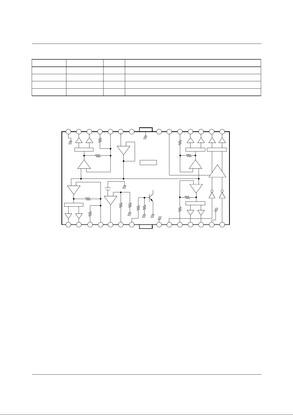
Internal Block Diagram
Pin Number Pin Name I/O Pin Function Description
25 DI4.2 I Tracking input 2
26 DO4.1 O Tracking output 1 (+)
27 DO4.2 O Tracking output 2 (−)
28 GND3 - Ground 3
+
−
Level
shift
Regulator
Mute
−
+
10k
10k
50k
10k
50k
+
−
10k
+
−
+
−
+
−
+
−
12 345 6 8 9 10 11 12 13
15161718192021
22232425262728
10k
TSD
+
−
Level
shift
Level
shift
Level
shift
10k
10k
10k
10k
10k
−
−
+
+
714
DO1.1
DO1.2
DI1.1
DI1.2
REB
REO
MUTE
GND1
DI5.1
DI2
DO2.1
DO2.2
GND2
DI5.2
GND3
DO4.2
DO4.1
DI4.2
DI4.1
VREF
LD CTL
DI3
DO3.2
DO3.1
DO5.2
DO5.1
+
−
+
−
COMP
Level
shift
V
CC2
FIN
(GND)
V
CC1
FIN
(GND)
2.5V
FAN8001D
4
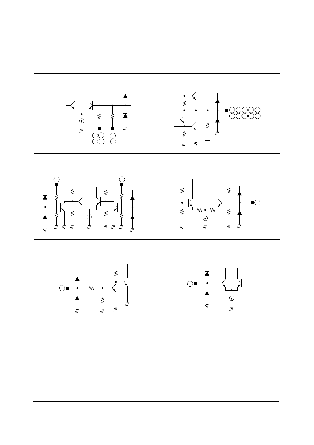
Equivalent Circuits
Driver input (Except for loading motor driver) Driver output
Loading motor driver input Loading motor speed control input
Mute input Bias input
4
10
2419325
2.5V
10k
1162171118122715
26
V
REF1
10k
20k
0.58k
9
14
50k
50k
50k
50k
50k
50k
50k
50k
20
50k
50k
50k 50k
50k
50k
7
50k
50k
50k
23
FAN8001D
5
Absolute Maximum Ratings (Ta = 25°°°°C)
NOTE:
1. When mounted on 76mm × 114mm × 1.57mm PCB (Phenolic resin material).
2. Power dissipation reduces 13.6mW / °C for using above Ta=25°C
3. Do not exceed Pd and SOA (Safe Operating Area).
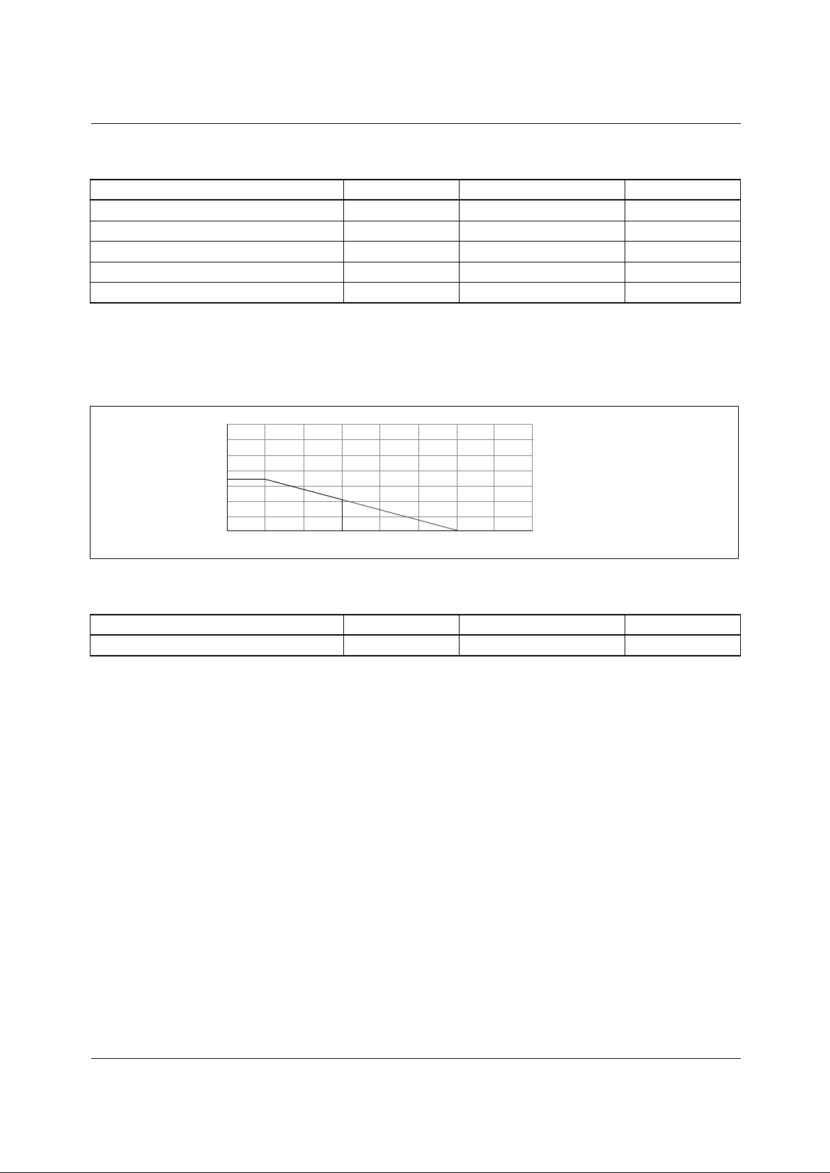
Power Dissipation Curve
Recommended Operating Condition (Ta = 25°°°°C)
Parameter Symbol Value Unit
Maximum supply voltage V
CC MAX
18 V
Power dissipation P
D
1.7
note
W
Operating temperature T
OPR
−25 ~ +75 °C
Storage temperature T
STG
−55 ~ +150 °C
Maximum current output I
OMAX
1A
Parameter Symbol Value Unit
Operating supply voltage V
CC
6 ~ 13.2 V
3,000
2,000
1,000
0
0 25 50 75 100 125 150 175
Pd (mW)
Ambient temperature, Ta [°C]
 Loading...