Fairchild Semiconductor FAN7563 Datasheet
FAN7563/FAN7564
Lithium-Ion Charger Controller
www.fairchildsemi.com
Features
• Constant Voltage & Constant Current Control
• Wide Operating Range of 2.5V ~ 16V
• Low-Side Source Return Current Sensing
• Externally Adjustable Charging Current Control
• Charging Current Monitoring
• Precision LDO Regulator Drive Ouptut (Adj)
(Only FAN7564)
• Error signals of Output Dropout (LDO)
(Only FAN7564)
• Current Limit (LDO)
( FAN7564 Only)
Description
The FAN7563/FAN7564 is designed for Lithium-ion battery
charger. This controls charging current and voltage of Lithium - ion battery as constant current and constant voltage
control IC and can be used for stand alone charger
(FAN7563) and micom interface charger(FAN7564). In
addition LDO regulator driving output which is integrated
within FAN75 64 enables to offer accurate reference voltag e
to power supply of micro controller, therefore, it features
increasing stability and efficiency of charger set as well as
minimizing external components of the set. Additionally,
FAN7563/FAN7564 provide the protection functions like
error flag, short circuit protection(LDO), and charging
current control disable.
8-SOP
1
14-SOP
1
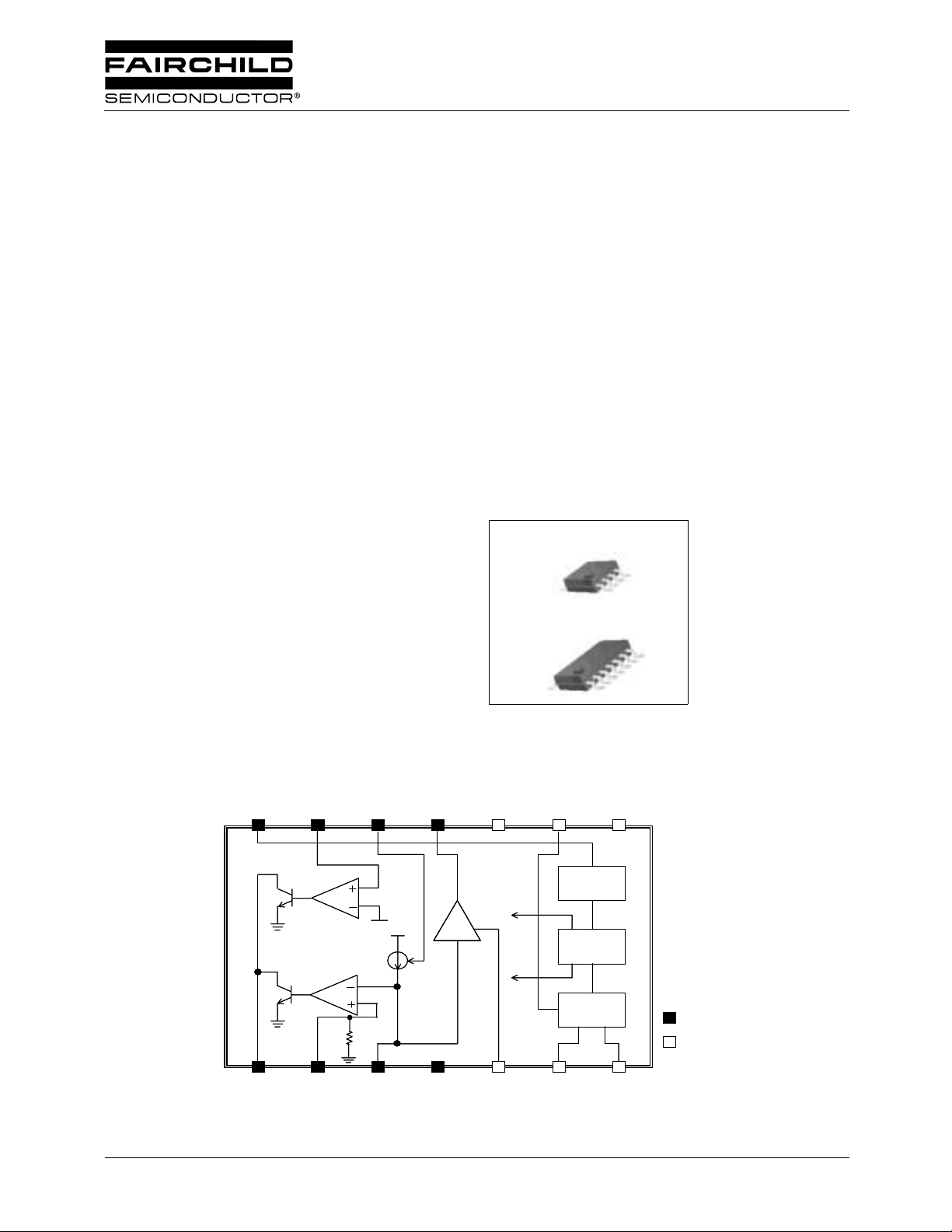
Internal Block Diagram
14(8)
14(8)
VCC
VCC
OUTPUT ISEN
OUTPUT ISEN
123 4
123 4
123 4
©2001 Fairchild Semiconductor Corporation
VSEN IREF
VSEN IREF
20kΩ
12(6)13(7)
12(6)13(7)
Vref(1.244V)
Vref(1.244V)
CS GND
CS GND
MONIT
MONIT
×5
×5×5
NC
NC
Reference
Reference
Internal
Internal
Bias
Bias
NC
NC
5
5
5
891011(5)
891011(5)
ERROR
ERROR
CHA-
CHA-
LDODRV
LDODRV
UVLO
UVLO
Reference
Reference
Bias
Bias
LDO
LDO
Drive
Drive
FB
67
67
67
FB
8SOP
8SOP
14SOP
14SOP
Rev. 1.0.3
FAN7563/FAN7564
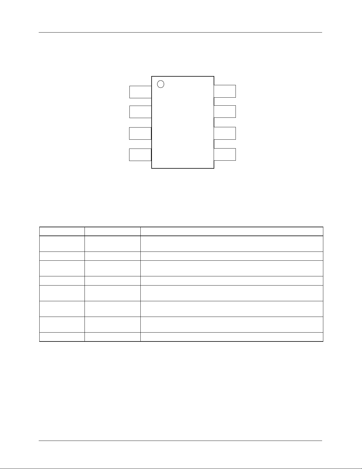
Pin Assignments
OUTPUT
ISEN
V
1
8
CC
FAN7563
VSEN
2
7
CS
GND
3
4
6
5
IREF
MONIT
Pin Definitions
Pin Number Pin Name Pin Function Descrition
1OUTPUT
2I
3CS
4 GND Ground
5MONIT
6I
7V
8V
SEN
REF
SEN
CC
Output pin for charging control. An external photocoupler is drived from
the output for constant voltage and constant current charging control.
Reference input for current amplifier.
Charging current sensing input . It is connected to a sense resistor
(system ground)
Charging current monitoring output. This pin is connected to a micro
controller and detects the amplified voltge derived from CS pin.
Reference current control input. The Amplifier reference current is
controlled according to the resistor which is connected to the pin I
Voltage sensing input for constant battery voltage control. It is normally
connected to the battery charger output through a resistor divider.
Power supply input. The typical operating voltage range is 2.5V to 16V.
REF
.
2
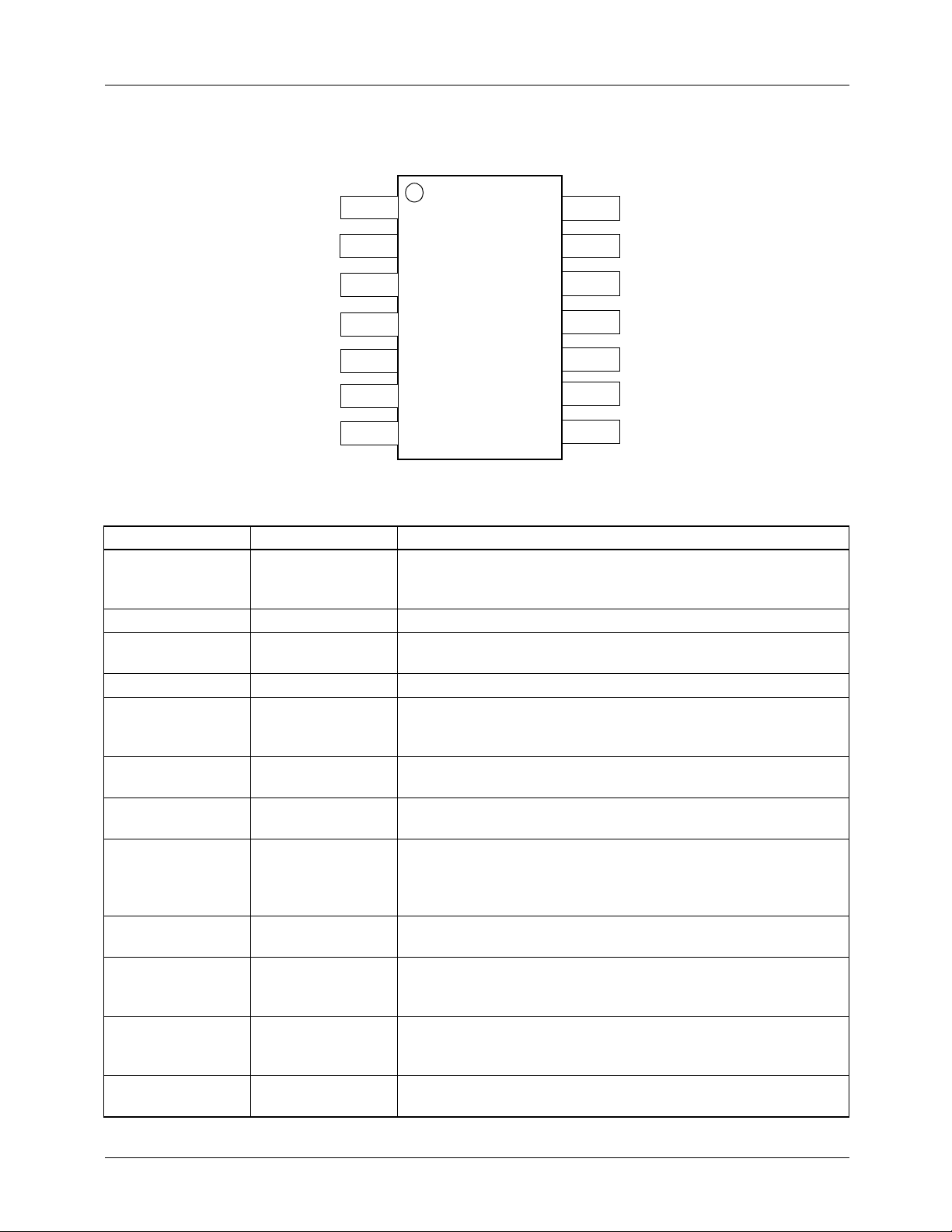
Pin Assignments (Continued)
FAN7563/FAN7564
CS
FB
1
2
3
4
5
6
7
Output pin for charging control. An external photocoupler is drived
from the output for constant voltage and constant current charging
control.
Constant current loop reference Input.
Charging current sensing input . It is connected to a sense resistor
(system ground)
Charging current monitoring feedback input. monitoring output
voltage can be changed by alternating the value of external resistor
which is connected to the pin6, CHA-
LDO output voltage sensing input. It is normally connected to the
LDO output through a resistor divider.
LDO driving output. This is connected to the base of external TR
(KSA539)
LDO dropout error flag. This keeps the error signal off until the bias
voltage for micro controller reaches the threshold voltage. Error
signal becomes ON when the voltage reaches 4.8V.
(With hysteresis 60mV)
Charging current monitoring output. This pin is connected to a micro
controller and detects the amplified voltage derived from CS pin.
Reference current control input. The Amplifier reference current is
controlled according to the resistor which is connected to the pin
I
REF
Voltage sensing input for constant Battery voltage control. It is
normally connected to the Battery charger output through a resistor
divider.
Power supply input. The typical operating voltage range is 2.5V to
16V.
FAN7564
.
14
13
12
11
10
9
8
V
CC
VSEN
IREF
MONIT
NC
ERROR
LDODRV
OUTPUT
ISEN
GND
NC
CHA-
Pin Definitions
Pin Number Pin Name Pin Function & Descrition
1OUTPUT
2I
3CS
4 GND Ground
6CHA-
7FB
8LDODRV
9 ERROR
11 MONIT
12 I
13 V
14 V
(Continued)
SEN
REF
SEN
CC
3
FAN7563/FAN7564
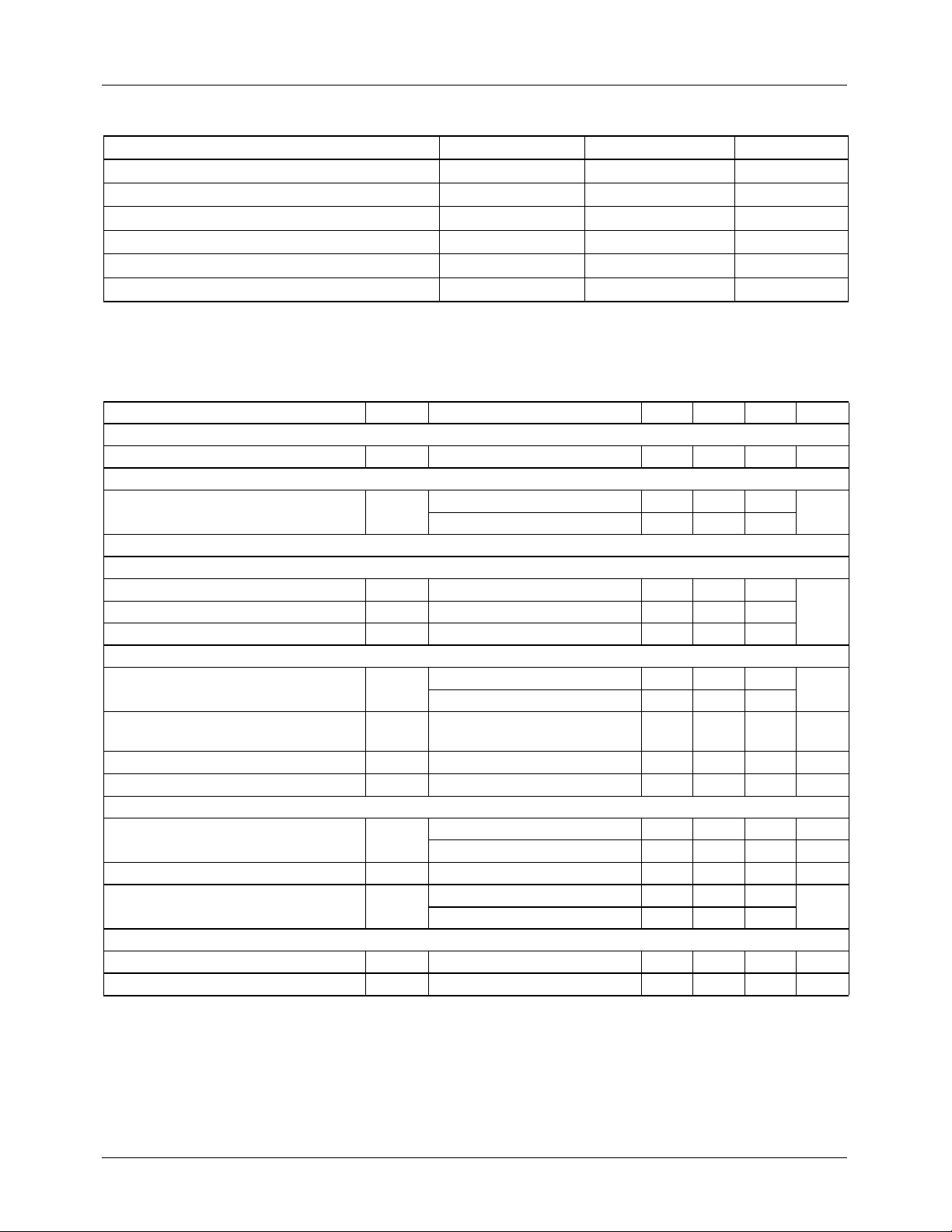
Absolute Maximum Ratings (Ta = 25°°°°C)
Parameter Symbol Value Unit
Supply Voltage V
CC
2.5 ~ 16 V
Ldodrv Sink Current Idrv 2 mA
Output Sink Current I
O
20 mA
Power Dissipation Pd 0.75 W
Operating Temperature Range Topr -25 ~ 85 °C
Storage Temperature Range Tstg -65 ~ 150 °C
Electrical Characteri sti c (FAN 7 563)
( Vcc = 6V, Ta= 25°C,for min/max values Ta is the operating juntion temperature range that applies(NOTE 1),
unless otherwise noted.))
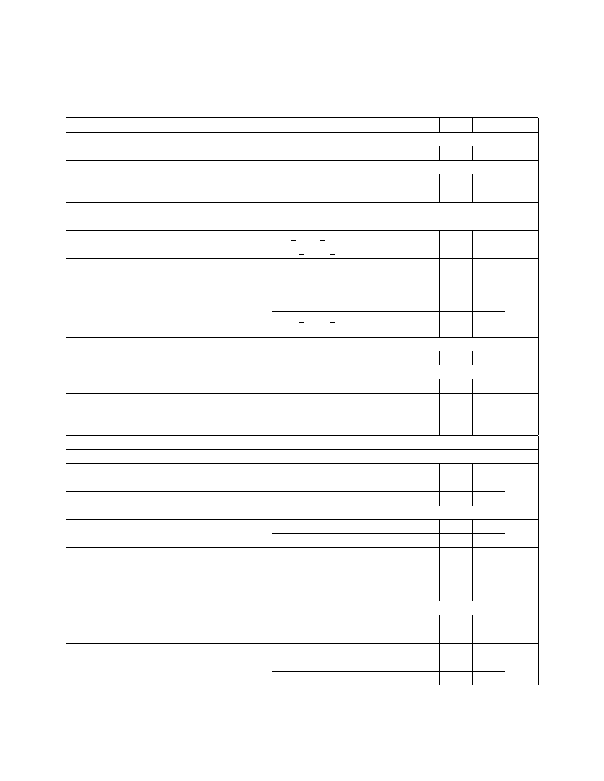
Parameter Symbol Conditions Min. Typ. Max. Unit
TOTAL DEVICE
Input Supply Current I
CC
REFERENCE SECTION
Reference voltage Vref
CONTROL PART
UVLO Section
High Threshold Voltage Vth(H) - - 2.5 2.6
Hysteresis 2 Vhys2 - - 0.1 -
VOLTAGE SENSE SECTION
Voltage Sense
Threshold Voltage
Threshold Voltage
Temperature Coefficient
Vvsen
∆Vvsen/
∆T
Input Bias Current Ii - - 40 - nA
Transconductance gm (V) - - 1 - S
CURRENT SENSE SECTION
Current Sense Threshold voltage Visen
Transconductance gm - - 1 - S
Current Reference Voltage Viref
OUTPUT SECTION
Output Sink Current I
Output Saturation Voltage Vsat I
VCC=6V, Iload=1mA, IO=0A - - 3 mA
=6V,Iload=50mA,Ta=25°C 1.23 1.245 1.26
V
CC
Full Temperature Range 1.22 1.245 1.27
= 6V, Ta = 25°C 1.23 1.245 1.26
V
CC
Full Temperature Range 1.22 1.245 1.27
-
= 6V, Ta=25°C -190 -200 -210 mV
V
CC
- ±0.01 - %/°C
Full Temperature Range - 0 - mV/°C
Rpin12=25KΩ, Ta=25°C 1.23 1.245 1.26
Full Temperature Range 1.22 1.245 1.27
O
=5mA - 200 400 mV
O
-5--mA
V
VLow Threshold Voltage Vth(L) - 2.3 2.4 -
V
V
NOTE:
1. Tested ambient temperature range for the FAN7563: Tlow = -25°C, Thigh=85°C
2.
1
S
--- -=
R
4
FAN7563/FAN7564
Electrical Characteristic (Continued) (FAN7564)
(VCC = 6V, Ta= 25°C,for min/max values Ta is the operating juntion temperature range that applies (NOTE 1),
unless otherwise noted.)
Parameter Symbol Conditions Min. Typ. Max. Unit
TOTAL DEVICE
Input Supply Current I
CC
REFERENCE SECTION
Reference voltage Vref
REGULATOR PART
EXTERNAL OUTPUT SECTION (NOTE2)
Line Regulation ∆Vr(Ii) 6V <
Load Regulation ∆Vr(I
Current Limit I
CL
Output Voltage V
INTERNAL DRIVE SECTION
LDODRV Sink Current Idrv V
ERROR COMPARATOR SECTION
Output Low Voltage V
High Threshold Voltage Vth - - 4.8 4.9 V
Low Threshold Voltage Vtl - 4.64 4.74 - V
Hysteresis1 Vhys1 - - 0.1 - mV
CONTROL PART
UVLO Section
High Threshold Voltage Vth(H) - - 2.5 2.6
Hysteresis 2 Vhys1 - - 60 -
VOLTAGE SENSE SECTION
Voltage Sense
Threshold Voltage
Threshold Voltage
Temperature Coefficient
Vvsen
∆Vvsen/
∆T
Input Bias Current Ii - - 40 - nA
Transconductance gm (V) - - 1 - S
CURRENT SENSE SECTION
Current Sense Threshold voltage Visen
Transconductance gm - - 1 - S
Current Reference Voltage Viref
VCC=6V, Iload=1mA, IO=0A - - 3 mA
=6V,Iload=50mA,Ta=25°C 1.23 1.245 1.26
V
CC
Full Temperature Range 1.22 1.245 1.27
VCC < 15V - - 0.5 %max
)1mA < Iload < 100mA - - 0.5 %max
O
VO=0V 110 - - mA
VCC=6V, Iload=50mA,
Ta=25°C
O
1mA <
Iload < 100mA
Full Temperature Range
=6V - - 2 mA
CC
VCC=(VO-0.5)V, IOL=500µA - 150 400 mV
OL
V
= 6V, Ta = 25°C 1.23 1.245 1.26
CC
4.95 5.0 5.05
4.88 5.0 5.12
Full Temperature Range 1.22 1.245 1.27
--±0.01 - %/°C
= 6V, Ta=25°C -190 -200 -210 mV
V
CC
Full Temperature Range - 0 - mV/°C
Rpin12=25KΩ, Ta=25°C 1.23 1.245 1.26
Full Temperature Range 1.22 1.245 1.27
V
VFull Temperature Range 4.9 5.0 5.1
VLow Threshold Voltage Vth(L) - 2.3 2.4 -
V
V
5
 Loading...