Fairchild Semiconductor FAN5250 Datasheet

www.fairchildsemi.com
FAN5250
Mobile Processor Core-Voltage Regulator
Features
• High efficiency over wide load range
• Non dissipative current-sense; uses MOSFET R
can use optional Current-Sense resistor for greater
precision
• Overcurrent protection
• Powerful drivers for N-Channel MOSFETs with adaptive
dead time
• Precision core voltage control
• Remote “Kelvin” sensing
• Summing current-mode control with programmable
Active Droop for Optimum Transient Response and
Lower Processor Power Dissipation
• 5-Bit Digital Output Voltage Selection
• Wide Range output voltage: 0.6 VDC to 1.0 VDC in
25mV Steps, and from 1.0 VDC to 1.75 VDC in 50mV
Steps
• “On-the-Fly” VID code change with programmable slew
rate
• Alternative input to set output voltage during start-up or
power saving modes
• Forced continuous conduction mode of operation
• Output voltage (Power-Good) monitor
• No negative core voltage on turn-off
• Over-Voltage, Under-Voltage and Over-Current fault
monitors
• Selectable 300/600kHz Switching Frequency
DS(ON)
or
Applications
• Transmeta’s Crusoe™ CPU core power
• Intel P3-M™ processor (IMVP-2)
Description
The FAN5250 is a single output power controller to power
mobile CPU cores. The FAN5250 includes a 5-bit digital-toanalog converter (DAC) that adjusts the core PWM output
voltage from 0.6VDC to 1.75VDC, and may be changed
during operation. Special measures are taken to allow the
output to transition with controlled slew rate to comply with
Transmeta’s LongRun™ and Intel’s P3-M Speed-Step™
requirements. The FAN5250 includes a precision reference,
and a proprietary architecture with integrated compensation
providing excellent static and dynamic core voltage regulation.
With nominal currents, the controller operates at a selectable
frequency of 300kHz or 600kHz. At light loads, when the
filter inductor current becomes discontinuous, the controller
operates in a hysteretic mode dramatically improving system
efficiency. The hysteretic mode of operation can be inhibited
by the FPWM
The FAN5250 monitors the output voltage and issues a
PGOOD (Power-Good) when soft start is completed and the
output is in regulation. A built-in over-voltage protection
(OVP) forces the lower MOSFET on to prevent output voltages from exceeding 1.9V. Undervoltage protection latches
the chip off when the output drops below 75% of the set
value. The PWM controller's overcurrent circuitry monitors
the converter load by sensing the voltage drop across the
lower MOSFET. The overcurrent threshold is set by an
external resistor. If precision overcurrent protection is
required, an optional external current-sense resistor may
be used.
control pin.
LongRun is a trademark of Transmeta Corporation.
REV. 1.1.6 3/12/03

FAN5250
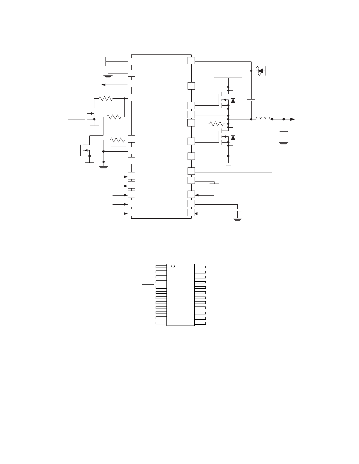
Typical Application
START
DSX
+5
PGOOD
R7
PVCC
AGND
ALTV
R8
ILIM
R5
FPWM
FREQ
VID0
VID1
VID2
VID3
VID4
24
15
12
11
10
1
3
6
FAN5250
5
7
9
8
18
13
19
20
21
23
22
16
17
4
14
2
BOOT
VIN (BATTERY)
VIN
HDRV
SW
ISNS
LDRV
PGND
VCORE+
N/C
EN
SS
VCC
+5
= 5 to 24V
Q1
Q2
+5
C
BOOT
L
OUT
V CORE
C
OUT
C
SS
Figure 1.
Pin Assignments
AGND
VCC
PGOOD
EN
FPWM
ALTV
FREQ
VID4
VID3
VID2
VID1
VID0
1
2
3
4
5
6
7
8
9
10
11
12
QSOP-24
Θ
= 90°C
JA
24
23
22
21
20
19
18
17
16
15
14
13
PVCC
LDRV
PGND
ISNS
SW
HDRV
BOOT
NC
VCORE+
ILIM
SS
VIN
2
REV. 1.1.6 3/12/03

FAN5250
+
Pin Description
Pin
Number Pin Name Pin Function Description
1 AGND Analog Ground . This is the signal ground reference for the IC. All voltage levels are
measured with respect to this pin.
2 VCC
3 PGOOD Power Good Flag. An open-drain output that will pull LOW when the core output is
4EN ENABLE. This pin enables IC operation when either left open, or pulled up to VCC.
5 FPWM Forced PWM mode. When logic low, inhibits the chip from entering hysteretic operating
6ALTV Alternative to VID. The IC will regulate to the voltage on this pin if it is below the highest
7 FREQ Frequency Set. Logic Low sets the operating frequency to 300Khz. High sets the
8–12 VID0–4 Voltage Identification Code . Input to VID DAC. Sets the output voltage according to the
13 VIN
14 SS
15 ILIM
16 V
17 NC
18 BOOT BOOT. The positive supply for the upper MOSFET driver. Connect as shown in Figure 1.
19 HDRV High-Side Drive. The high-side (upper) MOSFET driver output.
20 SW
21 ISNS
22 PGND Power Ground. The return for the low-side MOSFET driver.
23 LDRV Low-Side Drive. The low-side (lower) MOSFET driver output.
24 PVCC Power VCC. The positive supply for the lower MOSFET driver.
CORE
VCC. This pin powers the chip. The IC starts to operate when voltage on this pin exceeds
4.6V (UVLO rising) and shuts down when it drops below 4.3V (UVLO falling).
outside of a +25% –10% range of the VID reference voltage The PGOOD pin is kept high
during transitions between VID settings, Deep Sleep, and Reserved Mode transitions.
Toggling EN will also reset the chip after a latched fault condition.
mode.
VID voltage (1.75V). Such a requirement may occur during CPU initialization or during
some power saving modes. This pin has a 10 µ A current source, so that its voltage can be
programmed with a resistor to GND. See Alternative Voltage Programming on page 8 for
details.
frequency to 600Khz.
codes set as defined in Table 1.
Input Voltage from battery. This voltage is used by the oscillator for feed-forward
compensation of input voltage variation.
Soft Start. A capacitor from this pin to GND programs the slew rate of the converter
during initialization as well as in operation. This pin is used as the reference against which
the output is compared. During initialization, this pin is charged with a 25 µ A current
source. Once this pin reaches 0.5V, its function changes, and it assumes the value of the
voltage as set by the VID programming. The current driving this pin is then limited to
+500 µ A, that together with C
Current Limit. A resistor from this pin to GND sets the current limit.
VCORE Output Sense. This pin is the feedback from the VCORE output. Used for
regulation as well as PGOOD, under-voltage and over-voltage protection and monitoring.
No internal connection. While no connection is necessary, tying this pin to GND is
recommended to reduce coupled noise into pin 16 from pin 18.
Switching node. The return for the high-side MOSFET driver.
Current Sense Input. Monitors the voltage drop across the lower MOSFET or external
sense resistor for current feedback.
sets a controlled slew rate for VID code changes.
SS
REV. 1.1.6 3/12/03
3

FAN5250
Absolute Maximum Ratings
Absolute maximum ratings are the values beyond which the device may be damaged or have its useful life
impaired. Functional operation under these conditions is not implied
Parameter Min. Typ. Max. Units
VCC Supply Voltage 6.5 V
VIN 27 V
BOOT, SW, HDRV Pins 33 V
BOOT to SW 6.5 V
All Other Pins -0.3 VCC + 0.3 V
Junction Temperature (T
Storage Temperature -65 150 °C
Lead Soldering Temperature, 10 seconds 300 °C
) -10 150 °C
J
Recommended Operating Conditions
Parameter Conditions Min. Typ. Max. Units
Supply Voltage VCC 4.75 5 5.25 V
Supply Voltage VIN 5 24 V
Ambient Temperature (T
) –10 85 °C
A
4
REV. 1.1.6 3/12/03

FAN5250
Ω
Ω
Ω
Ω
Electrical Specifications
(VCC = 5V, VIN = 5V–24V, and T
unless otherwise noted)
Parameter Conditions Min. Typ. Max. Units
Power Supplies
VCC Current Operating, C
VIN Current Operating 12 20 µA
UVLO Threshold Rising VCC 4.3 4.65 4.75 V
Regulator / Control Functions
Output Voltage per Table 1. Output
Initial Accuracy -1 1 % VID
Static Load Regulation -2 2 % VID
Error Amplifier Gain 86 dB
Error Amplifier GBW 2.7 MHz
Error Amplifier Slew Rate 1 V/µS
ILIM Voltage R
Over-voltage Threshold 1.9 1.95 2.0 V
Over-voltage Protection Delay 1.6 3.2 µS
Under-voltage Shutdown Disabled during VID code
Under-voltage Delay 1.2 1.6 µS
EN, input threshold Logic LOW 1.2 V
Output Drivers
HDRV Output Resistance Sourcing 3.8 5
LDRV Output Resistance Sourcing 3.8 5
Oscillator
Frequency FREQ = HIGH 255 300 345 KHz
Ramp Amplitude, pk-pk VIN = 16V 2 V
Ramp Offset 0.5 V
Ramp Gain Ramp amplitude
Reference, DAC and Soft-Start
VID input threshold Logic LOW 1.21 V
VID pull-up current to internal 2.5V reference 12 µA
DAC output accuracy -1 1 %
= recommended operating ambient temperature range using circuit of Figure 1,
A
= 10pF 2.7 3.2 mA
L
Shut-down (EN = 0) 6 30 µA
Shut-down (EN = 0) 1 µA
Falling 4.1 4.35 4.45 V
0.6 1.75 V
Voltage VID
= 30K Ω
ILIM
change
Logic HIGH 2 V
Sinking 1.6 3
Sinking 0.8 1.5
FREQ = LOW 510 600 690 KHz
VIN
Logic HIGH 1.62 V
0.89 0.91 V
72 75 78 % VID
125 mV/V
REV. 1.1.6 3/12/03
5

FAN5250
Electrical Specifications
(VCC = 5V, VIN = 5V–24V, and T
(continued)
= recommended operating ambient temperature range using circuit of Figure 1,
A
unless otherwise noted)
Parameter Conditions Min. Typ. Max. Units
Soft Start current (I
) at start-up, V
SS
at start-up, 1.75 > V
< 0.5 20 26 32 µA
SS
> 0.5 350 500 650 µA
SS
ALTV Current Source 9.5 10 10.5 µA
ALTV to VID mode threshold 1.71 1.75 1.78 V
PGOOD
VCORE Upper Threshold 123 127 % VID
VCORE Lower Threshold Falling Edge 77 81 % VID
Rising Edge 87 94 % VID
PGOOD Output Low IPGOOD = 4mA 0.5 V
Leakage Current V
EN
4
5
13
7
16
14
3
FPWM
VIN
FREQ
VCORE+
SS
PGOOD
SS
HYST
OSC
DAC and
Soft Start
OVP
RAMP
CLK
SR
EA
POR/UVLO
Q
PWM
DTY CYC
CLAMP
= 5V 1 µA
PULLUP
5V
RAMP
Σ
VDD
7
FPWM
HYST
ADAPTIVE
GATE
CONTROL LOGIC
PWM
PWM/HYST
ILIM det.
CURRENT PROCESSING
I
OUT
S/H
MODE
15
VDD
ILIM
R5
18
19
20
21
4
5
BOOT
HDRV
SW
LDRV
PGND
ISNS
Q1
Q2
R
VIN
SENSE
C
BOOT
L
OUT
V CORE
C
OUT
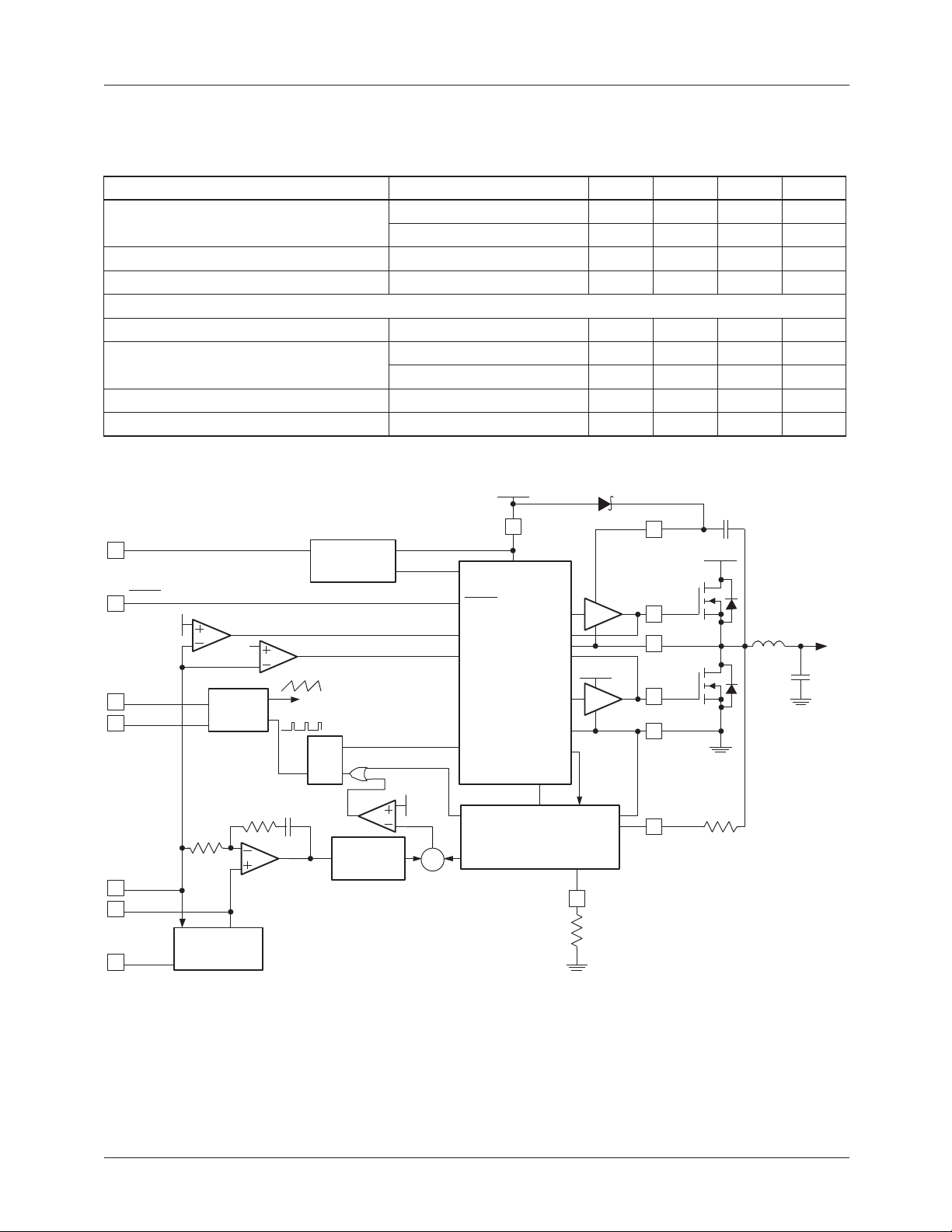
Figure 2. IC Block Diagram
6
REV. 1.1.6 3/12/03
 Loading...