www.fairchildsemi.com
FAN5240
Multi-Phase PWM Controller for AMD Mobile
Athlon
TM
and Duron
TM
Features
• CPU Core power: 0.925V to 2.0V output range
• ±1% reference precision over temperature
• Dynamic voltage setting with 5-bit DAC
• 5V to 24V input voltage range
• 2 phase interleaved switching
• Active droop to reduce output capacitor size
• Differential remote voltage sense
• High efficiency:
>90% efficiency over wide load range
>80% efficiency at light load
• Excellent dynamic response with Voltage Feed-Forward
and Average Current Mode control
• Dynamic duty cycle clamp minimizes inductor current
build up
• Lossless current sensing on low-side MOSFET or
Precision current sensing using sense resistor
• Fault protections: Over-voltage, Over-current, and
Thermal Shut-down
• Controls: Enable, Forced PWM, Power Good, Power
Good Delay
• QSOP28, TSSOP28
Applications
• AMD Mobile Athlon CPU V
• AMD Mobile Duron CPU V
CORE
CORE
Regulator
Regulator
General Description
The FAN5240 is a single output 2-Phase synchronous buck
controller to power AMD’s mobile CPU core. The FAN5240
includes a 5-bit digital-to-analog converter (DAC) that
adjusts the core PWM output voltage from 0.925VDC to
2.0VDC, which may be changed during operation. Special
measures are taken to allow the output to transition with
controlled slew rate to comply with AMD’s Power Now
technology. The FAN5240 includes a precision reference,
and a proprietary architecture with integrated compensation
providing excellent static and dynamic core voltage regulation. The regulator includes special circuitry which balances
the 2 phase currents for maximum efficiency.
At light loads, when the filter inductor current becomes
discontinuous, the controller operates in a hysteretic mode,
dramatically improving system efficiency. The hysteretic
mode of operation can be inhibited by the FPWM control
pin.
The FAN5240 monitors the output voltage and issues a
PGOOD (Power-Good) when soft start is completed and the
output is in regulation. A pin is provided to add delay to
PGOOD with an external capacitor.
A built-in over-voltage protection (OVP) forces the lower
MOSFET on to prevent the output from exceeding a set
voltage. The PWM controller's overcurrent circuitry monitors the converter load by sensing the voltage drop across the
lower MOSFET. The overcurrent threshold is set by an external resistor. If precision overcurrent protection is required,
an optional external current-sense resistor may be used.
REV. 1.1.7 8/29/02

FAN5240 PRODUCT SPECIFICATION
Typical Application
VIN (BATTERY)
= 5 to 24
+5
C3
C4
+5
R1
PGOOD
C5
FPWM
C11
0
C1
DELAY
R4
AGND
V
VCC
VID0
VID
VID
VID
VID
ILIM
EN
SS
VI
N
21
28
Phase 1
19
14
12
11
1
10
2
9
3
8
4
7
20
16
13
15
Phase 2
25
24
23
27
26
22
18
17
3
C9
4
5
1
2
6
BOOT1
Q1
HDRV
1
1
SW
Q2
LDRV
1
1
PGND
ISNS1
VCORE +
VCORE D
2
BOOT
2
HDRV
SW
2
Q5
2
LDRV
PGND2
ISNS2
R6
VIN
Q4
C1
C7
C8
Q3
C12
C13C14C16
D1
C6
Q6
C2
D2
+5
R2
C15
+5
L2L1
R3
V
CORE
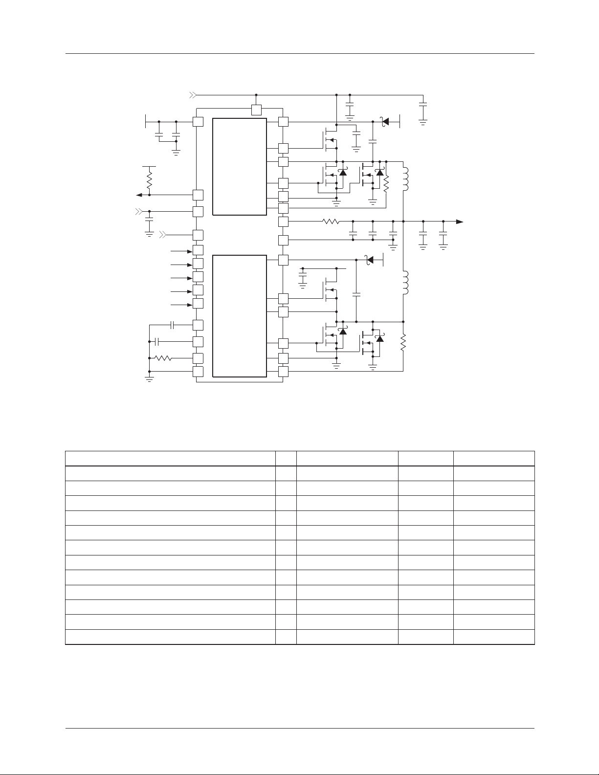
Figure 1. AMD Mobile Athlon/Duron CPU Core Supply
Table 1. BOM for Figure 1
Description Qty Ref. Vendor Part Number
Capacitor 22µF, Ceramic X7R 25V 2 C1, C2 TDK
Capacitor 1µF, Ceramic 3 C3,C7,C9 Any
Capacitor 0.1µF, Ceramic 6 C4–C6, C8, C11, C12 Any
Capacitor 0.22µF, Ceramic 1 C10 Any
Capacitor 270µF, 2V, ESR 15m Ω
4 C13–C16 Panasonic EEFUE0D271R
10K Ω , 5% Resistor 2 R1 Any
1K Ω , 1% Resistor 1 R2, R3, R6 Any
56.2K Ω , 1% Resistor 2 R4 Any
Schottky Diode 40V 2 D1, D2 Fairchild MBR0540
Inductor 1.6µH, 20A, 2.4m Ω
N-Channel SO-8 MOSFET, 11m Ω
N-Channel SO-8 SyncFET™ MOSFET, 6m Ω
1 L1, L2 Panasonic ETQP6F0R8LFA
1 Q1, Q4 Fairchild FDS6694
1 Q2, Q3, Q5, Q6 Fairchild FDS6676S
2
REV. 1.1.7 8/29/02

PRODUCT SPECIFICATION FAN5240
Pin Configuration
LDRV2
PGND2
BOOT2
HDRV2
SW2
ISNS2
VID4
VID3
VID2
VID1
VID0
FPWM
ILIM
1
2
3
4
5
6
7
FAN5240
8
9
10
11
12
13
EN
14
QSOP-28 or TSSOP-28
VCC
28
LDRV1
27
PGND1
26
BOOT1
25
HDRV1
24
SW1
23
ISNS1
22
VIN
21
SS
20
PGOOD
19
VCORE+
18
VCORED
17
DELAY
16
AGND
15
θJA = 90°C/W
Pin Definitions
Pin
Number
1
27
2
26
3
25
4
24
5
23
6
22
7 - 11 VID4 -
12 FPWM Forced PWM mode. When logic high, inhibits the chip from entering hysteretic operating
13 ILIM Current Limit. A resistor from this pin to GND sets the current limit.
14 EN
15 AGND Analog Ground. This is the signal ground reference for the IC. All voltage levels are
16 DELAY Power Good / Over-Current Delay. A capacitor to GND on this pin delays the PGOOD
18
17
19 PGOOD Power Good Flag. An open-drain output that will pull LOW when the core output below
Pin
Name
LDRV2
LDRV1
PGND2
PGND1
BOOT2
BOOT1
HDRV2
HDRV1
SW2
SW1
ISNS2
ISNS1
VID0
VCORE+
VCORE–
Pin Function Description
Low-Side Drive. The low-side (lower) MOSFET driver output.
Power Ground. The return for the low-side MOSFET driver.
BOOT. The positive supply for the upper MOSFET driver. Connect as shown in Figure 1.
High-Side Drive. The high-side (upper) MOSFET driver output.
Switching node. The return for the high-side MOSFET driver.
Current Sense input. Monitors the voltage drop across the lower MOSFET or external
sense resistor for current feedback.
Voltage Identification Code. Input to VID DAC. Sets the output voltage according to the
codes set as defined in Table 2. These inputs have 1 µ A internal pull-up.
mode. If tied low, hysteretic mode will be allowed.
ENABLE. This pin enables IC operation when either left open, or pulled up to VCC.
Toggling EN will also reset the chip after a latched fault condition.
measured with respect to this pin.
from going high as well delaying the over-current shutdown.
VCORE Output Sense. Differential sensing of the output voltage. Used for regulation as
well as PGOOD, under-voltage and over-voltage protection and monitoring. A resistor in
series with this VCORE+ sets the output voltage droop.
825mV. PGOOD delays its low to high transition for a time determined by CDELAY when
VCORE rises above 875mV.
REV. 1.1.7 8/29/02
3

FAN5240 PRODUCT SPECIFICATION
Pin Definitions
Pin
Number
20 SS
21 VIN
28 VCC VCC. This pin powers the chip. The IC starts to operate when voltage on this pin exceeds
Pin
Name
(continued)
Pin Function Description
Soft Start. A capacitor from this pin to GND programs the slew rate of the converter during
initialization as well as in operation. This pin is used as the reference against which the
output is compared. During initialization, this pin is charged with a 25 µ A current source.
Once this pin reaches 0.5V, its function changes, and it assumes the value of the voltage
as set by the VID programming. The current driving this pin is then limited to ±500 µ A, that
together with C
Input voltage from battery. This voltage is used by the oscillator for feed-forward
compensation of input voltage variation.
4.6V (UVLO rising) and shuts down when it drops below 4.3V (UVLO falling).
sets a controlled slew rate for VID code changes.
SS
Absolute Maximum Ratings
Absolute maximum ratings are the values beyond which the device may be damaged or have its useful life
impaired. Functional operation under these conditions is not implied.
Parameter Min. Typ. Max. Units
VCC Supply Voltage: 6.5 V
VIN 27 V
BOOT, SW, HDRV Pins 33 V
BOOT to SW 6.5 V
All Other Pins –0.3 VCC+0.3 V
Junction Temperature (T
Storage Temperature –65 150 °C
Lead Soldering Temperature, 10 seconds 300 °C
) –10 150 °C
J
Recommended Operating Conditions
Parameter Conditions Min. Typ. Max. Units
Supply Voltage VCC 4.75 5 5.25 V
Supply Voltage VIN 6 24 V
Ambient Temperature (T
4
) –20 85 °C
A
REV. 1.1.7 8/29/02

µ
µ
µ
µ
µ
Ω
Ω
Ω
Ω
µ
µ
PRODUCT SPECIFICATION FAN5240
µ
Electrical Specifications
(VCC = 5V, VIN = 6V–24V, and T
unless otherwise noted.)
Parameter
Power Supplies
VCC Current Operating, C
VIN Current Operating 25
UVLO Threshold Rising VCC 4.3 4.45 4.6 V
Regulator / Control Functions
Output voltage per Table 2 0.925 2.00 V
Error Amplifier Gain 86 dB
Error Amplifier GBW 2.7 MHz
Error Amplifier Slew Rate 1 V/ µ S
VCORE+ Input Current 25 30 35
ILIM Voltage R
ILIM T
HOLDOFF
Over-voltage Threshold 2.2 2.35 2.5 V
Over-voltage Protection delay 2
EN, input threshold Logic LOW 0.8 V
Phase to Phase current mismatch IC contribution only
Over-Temperature Shut-down 150 °C
Over-Temperature Hysteresis 25 °C
Output Drivers
(note 1)
HDRV Output Resistance Sourcing 3.8 5
LDRV Output Resistance Sourcing 3.8 5
Oscillator
Frequency 255 300 345 KHz
Ramp Amplitude, pk–pk VIN = 16V 2 V
Ramp Offset 0.5 V
Ramp Gain 125 mV/V
Reference, DAC and Soft-Start
VID input threshold Logic LOW 0.8 V
VID pull-up current to VCC 1
DAC output accuracy –11%
Soft Start Charging current (I
Note 1: Guaranteed by slew rate testing.
= recommended operating ambient temperature range using circuit of Figure 1,
A
Conditions Min. Typ. Max. Units
= 10pF 2 mA
L
Shut-down (EN=0) 1 10
Shut-down (EN=0) 1
Falling VCC 3.8 3.95 4.10 V
ILIM
C
DELAY
= 30K Ω
= 22nF 1.16 mS
0.89 0.91 V
Logic HIGH 2 V
±5 %
Guaranteed by design
Sinking 1.6 3
Sinking 0.8 1.5
RampAmplitude
----------------------------------------------
V
IN
Logic HIGH 2.0 V
)V
SS
< 90% of Programmed output 20 27 34
SS
V
> 90% of Programmed output 350 500 650
SS
A
A
A
A
S
A
A
A
REV. 1.1.7 8/29/02
5

µ
FAN5240 PRODUCT SPECIFICATION
Electrical Specifications
Parameter
(continued)
Conditions Min. Typ. Max. Units
PGOOD
VCORE Lower Threshold Falling Edge 800 825 850 mV
Rising Edge 850 875 900 mV
PGOOD Output Delay Low to High, C
PGOOD Output Low I
Leakage Current V
EN
POR/UVLO
SS
'
VOUT
PGOOD
VIN
EA1
ISNS1+ISNS2
5
VCORE+
30mA
VCORE-
DAC
Soft Start &
OVP
OSC
RAMP CLK
DUTY
CYCLE
CLAMP
ISNS1-ISNS2
A1
= 4mA 0.5 V
PGOOD
= 5V 1
PULLUP
HYST
Q
SR
PWM
A2
ISNS2-ISNS1
= 22nF 12 mS
DELAY
5V
VDD
HYST
FPWM
PWM
A
VOUT '
B
TO PH 2
MODULATOR
PWM/HYST
ILIM
MODE
det.
CURRENT
PROCESSING
ISNS1
ISNS2
S/H
VDD
I
LIM
ILIM
R
BOOT
HDRV
SW
LDRV
PGND
ISNS1
ISNS2
Q1
Q2
R
R
C
VIN
SENSE1
SENSE2
BOOT
VCORE
L
OUT
+
C
OUT
A
1K
R6
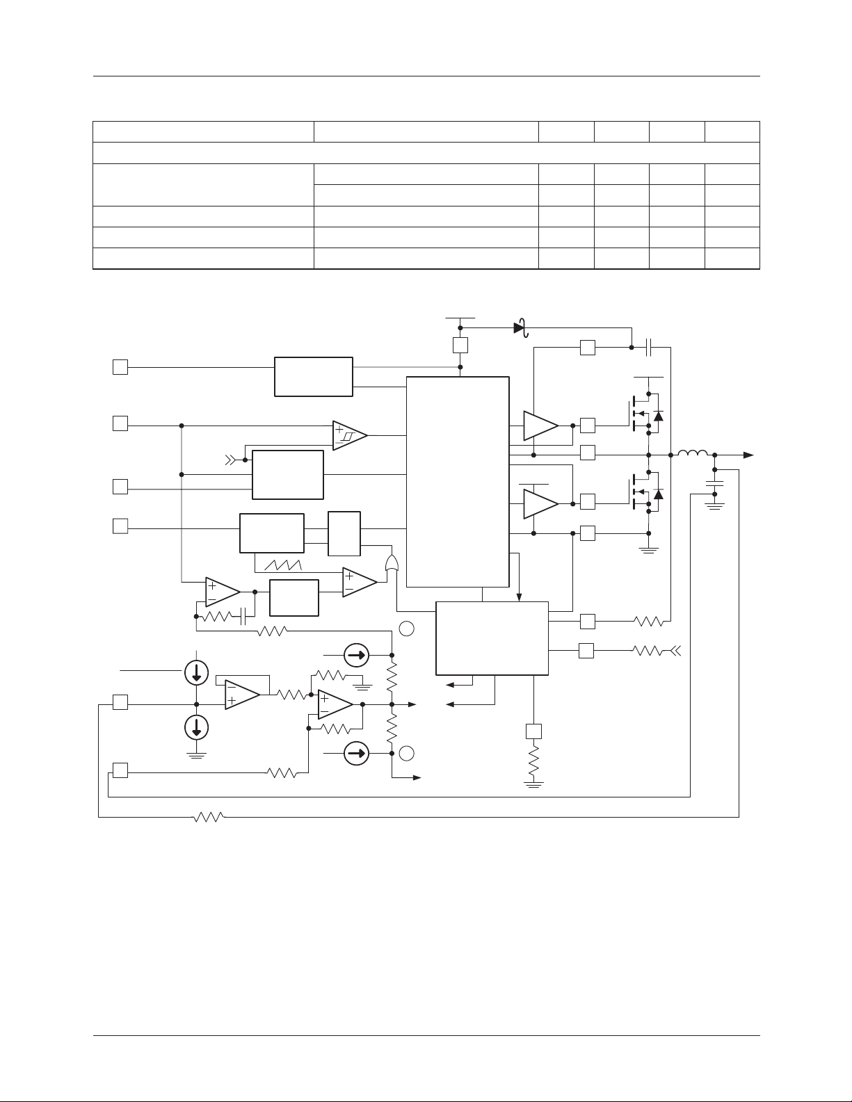
Figure 2. IC Block Diagram
6
REV. 1.1.7 8/29/02
 Loading...