

Fairchild Semiconductor FAN5236 Datasheet

www.fairchildsemi.com
FAN5236
Dual Mobile-Friendly DDR / Dual-output PWM Controller
Features
• Highly flexible dual synchronous switching PWM
controller includes modes for:
– DDR mode with in-phase operation for reduced
channel interference
– 90˚ phase shifted two-stage DDR Mode for reduced
input ripple
– Dual Independent regulators 180° phase shifted
• Complete DDR Memory power solution
–V
Tracks VDDQ/2
TT
– VDDQ/2 Buffered Reference Output
• Lossless current sensing on low-side MOSFET or
precision over-current using sense resistor
•V
Under-voltage Lockout
CC
• Converters can operate from +5V or 3.3V or Battery
power input (5 to 24V)
• Excellent dynamic response with Voltage Feed-Forward
and Average Current Mode control
•Power-Good Signal
• Also supports DDR-II and HSTL
• Light load Hysteretic mode maximizes efficiency
• QSOP28, TSSOP28
Applications
• DDR V
• Mobile PC dual regulator
• Server DDR power
• Hand-Held PC power
DDQ
and V
voltage generation
TT
General Description
The FAN5236 PWM controller provides high efficiency and
regulation for two output voltages adjustable in the range
from 0.9V to 5.5V that are required to power I/O, chip-sets,
and memory banks in high-performance notebook computers, PDAs and Internet appliances. Synchronous rectification
and hysteretic operation at light loads contribute to a high
efficiency over a wide range of loads. The hysteretic mode of
operation can be disabled separately on each PWM converter
if PWM mode is desired for all load levels. Efficiency is even
further enhanced by using MOSFET’s R
sense component.
Feed-forward ramp modulation, average current mode control scheme, and internal feedback compensation provide
fast response to load transients. Out-of-phase operation with
180 degree phase shift reduces input current ripple. The controller can be transformed into a complete DDR memory
power supply solution by activating a designated pin. In
DDR mode of operation one of the channels tracks the output voltage of another channel and provides output current
sink and source capability — features essential for proper
powering of DDR chips. The buffered reference voltage
required by this type of memory is also provided. The
FAN5236 monitors these outputs and generates separate
PGx (power good) signals when the soft-start is completed
and the output is within ±10% of its set point. A built-in
over-voltage protection prevents the output voltage from
going above 120% of the set point. Normal operation is automatically restored when the over-voltage conditions go
away. Under-voltage protection latches the chip off when
either output drops below 75% of its set value after the softstart sequence for this output is completed. An adjustable
over-current function monitors the output current by sensing
the voltage drop across the lower MOSFET. If precision current-sensing is required, an external current-sense resistor
may optionally be used.
DS(ON)
as a current
REV. 1.1.7 4/4/03
PRODUCT SPECIFICATION FAN5236
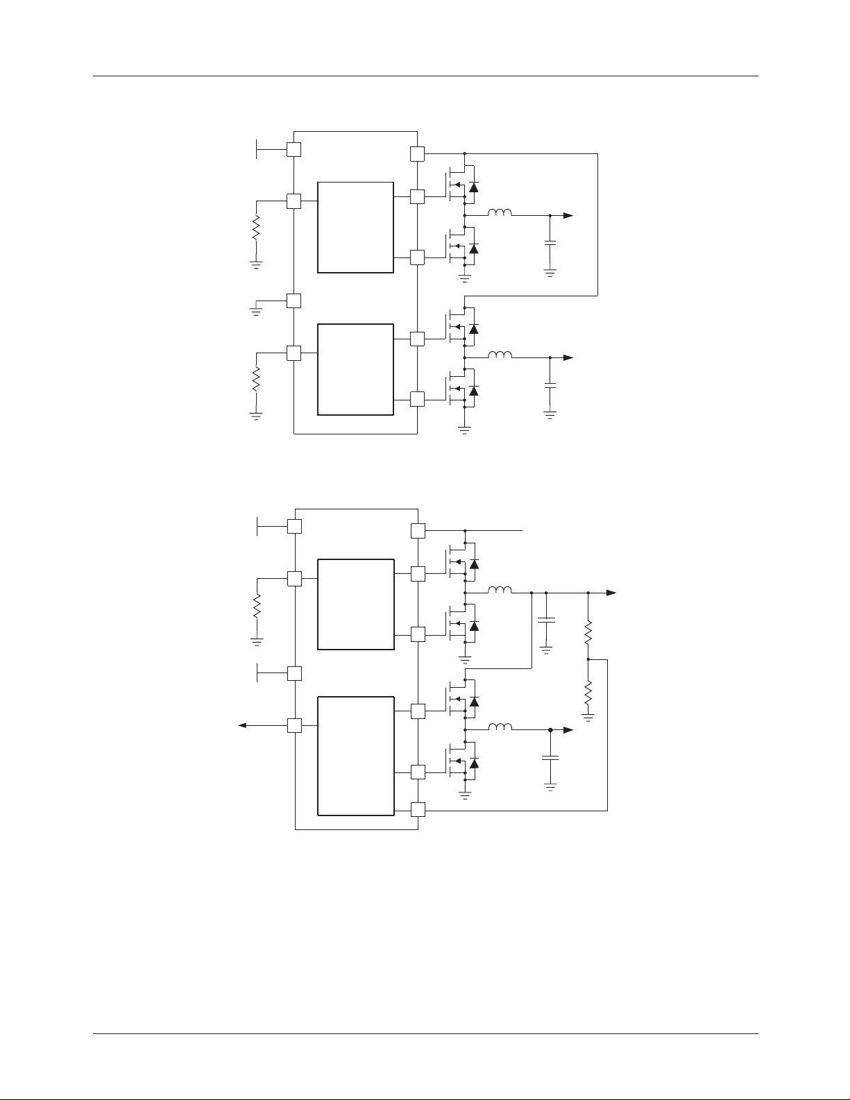
Generic Block Diagrams
VCC
+5
ILIM1
R
DD
ILIM2/
2
REF
FAN5236
PWM 1
PWM 2
VIN (BATTERY)
= 5 to
24V
Q1
OUT1
OUT2
VOUT1
= 2.
VOUT2
= 1.
L
Q2
Q3
L
Q4
5V
8V
C
OUT1
C
OUT2
Figure 1. Dual output regulator
VCC
+5
ILIM1
FAN5236
PWM 1
VIN (BATTERY)
= 5 to 24V
Q1
L
OUT1
Q2
VDDQ
= 2.
C
OUT1
5V
R
DDR
+5
PG2/REF
1.
25V
PWM 2
ILIM2/REF2
Q3
Q4
OUT2
VTT =
VDDQ
/2
C
L
R
OUT2
Figure 2. Complete DDR Memory Power Supply
2
REV. 1.1.7 4/4/03
FAN5236 PRODUCT SPECIFICATION
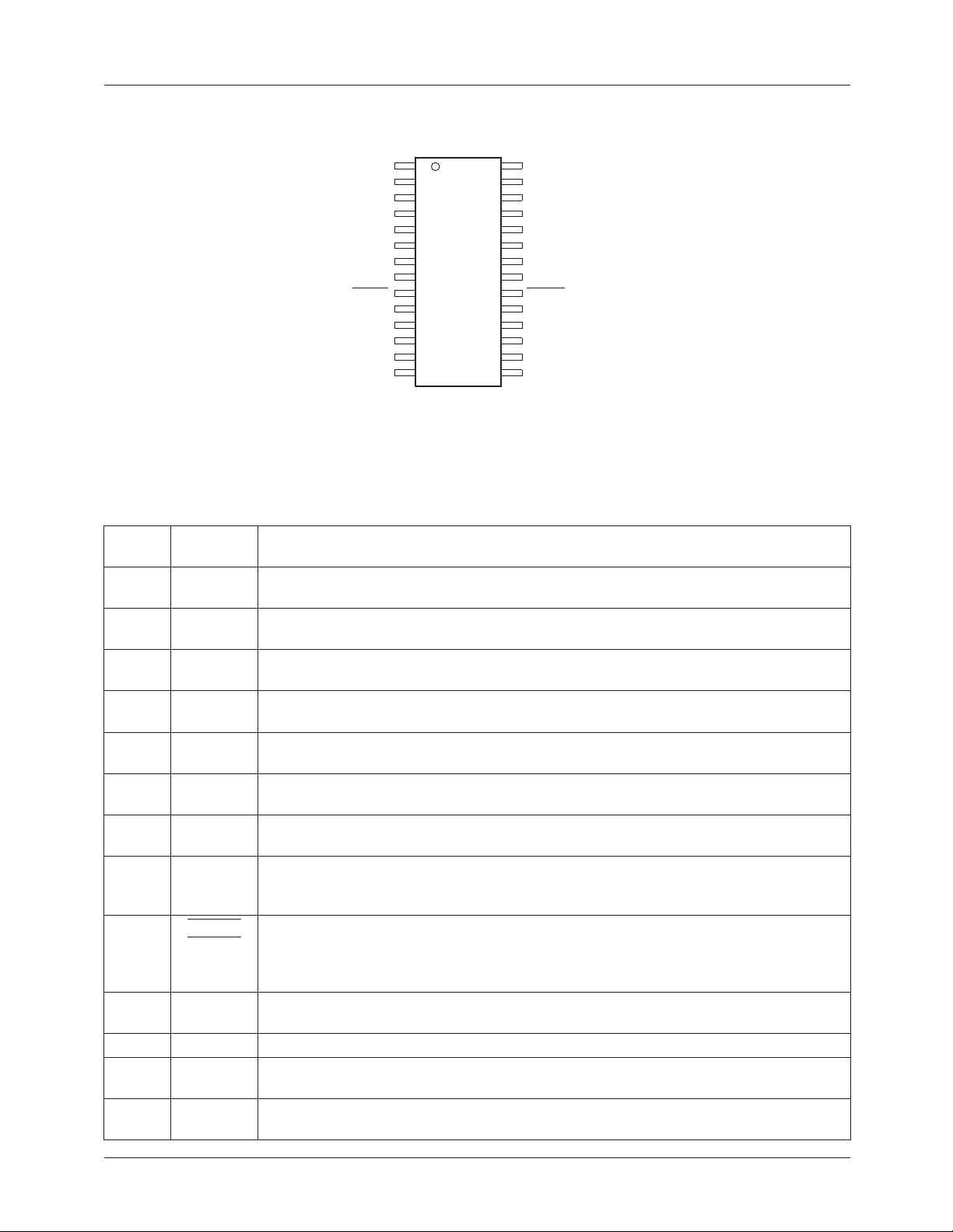
Pin Configurations
Pin Definitions
Pin
Number
1
2
27
3
26
4
25
5
24
6
23
7
22
8
21
9
20
10
19
11 ILIM1
12
17
13 DDR
Pin Name Pin Function Description
AGND
LDRV1
LDRV2
PGND1
PGND2
SW1
SW2
HDRV1 High-Side Drive. High-side (upper) MOSFET driver output. Connect to gate of high-side
BOOT1
BOOT2
ISNS1
ISNS2
EN1
EN2
FPWM1
FPWM2
VSEN1
VSEN2
SS1
SS2
AGND
LDRV1
PGND1
SW1
HDRV1
BOOT1
ISNS1
EN1
FPWM1
VSEN1
ILIM1
SS1
DDR
VIN
1
2
3
4
5
6
7
FAN5236
8
9
10
11
12
13
14
QSOP-28 or TSSOP-28
28
27
26
25
24
23
22
21
20
19
18
17
16
15
VCC
LDRV2
PGND2
SW2
HDRV2
BOOT2
ISNS2
EN2
FPWM2
VSEN2
ILIM2/REF2
SS2
PG2/REF2OUT
1
PG
θJA = 90°C/W
Analog Ground. This is the signal ground reference for the IC. All voltage levels are
measured with respect to this pin.
Low-Side Drive. The low-side (lower) MOSFET driver output. Connect to gate of low-side
MOSFET.
Power Ground. The return for the low-side MOSFET driver. Connect to source of low-
side MOSFET.
Switching node. Return for the high-side MOSFET driver and a current sense input.
Connect to source of high-side MOSFET and low-side MOSFET drain.
MOSFET.
BOOT. Positive supply for the upper MOSFET driver. Connect as shown in Figure 3.
Current Sense input. Monitors the voltage drop across the lower MOSFET or external
sense resistor for current feedback.
Enable . Enables operation when pulled to logic high. Toggling EN will also reset the
regulator after a latched fault condition. These are CMOS inputs whose state is
indeterminate if left open.
Forced PWM mode. When logic low, inhibits the regulator from entering hysteretic mode.
Otherwise tie to VOUT. The regulator uses VOUT on this pin to ensure a smooth
transition from Hysteretic mode to PWM mode. When VOUT is expected to exceed VCC,
tie to VCC.
Output Voltage Sense. The feedback from the outputs. Used for regulation as well as
PG, under-voltage and over-voltage protection and monitoring.
Current Limit 1. A resistor from this pin to GND sets the current limit.
Soft Start. A capacitor from this pin to GND programs the slew rate of the converter
during initialization. During initialization, this pin is charged with a 5 µ A current source.
DDR Mode Control. High = DDR mode. Low = 2 separate regulators operating 180° out
of phase.
REV. 1.1.7 4/4/03
3
PRODUCT SPECIFICATION FAN5236
Pin Definitions
14
15 PG1
16 PG2 /
18 ILIM2 /
28 VCC
VIN
REF2OUT
REF2
(continued)
Input Voltage. Normally connected to battery, providing voltage feed-forward to set the
amplitude of the internal oscillator ramp. When using the IC for 2-step conversion from 5V
input, connect through 100K to ground, which will set the appropriate ramp gain and
synchronize the channels 90˚ out of phase.
Power Good Flag. An open-drain output that will pull LOW when VSEN is outside of a
±10% range of the 0.9V reference.
Power Good 2. When not in DDR Mode: Open-drain output that pulls LOW when the
VOUT is out of regulation or in a fault condition
Reference Out 2. When in DDR Mode, provides a buffered output of REF2. Typically
used as the VDDQ/2 reference.
Current Limit 2. When not in DDR Mode, A resistor from this pin to GND sets the current
limit.
Reference for reg #2 when in DDR Mode. Typically set to VOUT1 / 2.
VCC. This pin powers the chip as well as the LDRV buffers. The IC starts to operate when
voltage on this pin exceeds 4.6V (UVLO rising) and shuts down when it drops below 4.3V
(UVLO falling).
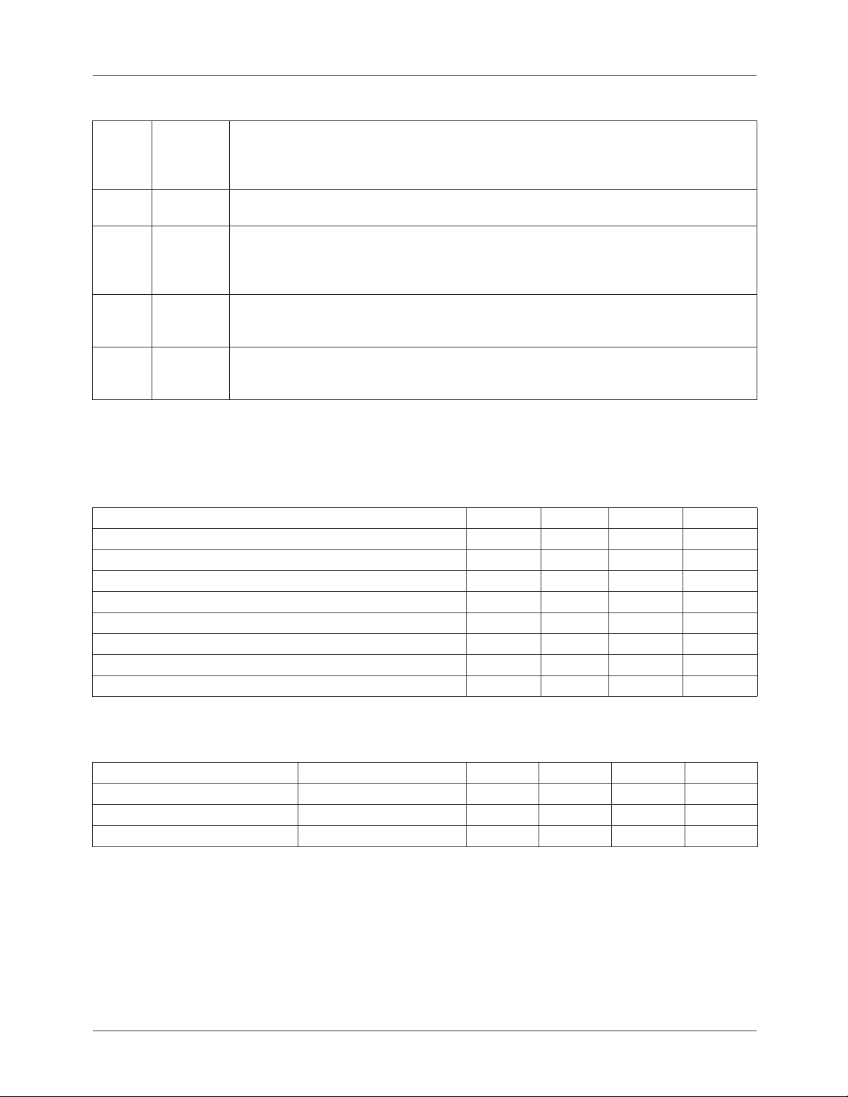
Absolute Maximum Ratings
Absolute maximum ratings are the values beyond which the device may be damaged or have its useful life
impaired. Functional operation under these conditions is not implied.
Parameter Min. Typ. Max. Units
VCC Supply Voltage: 6.5 V
VIN 27 V
BOOT, SW, ISNS, HDRV 33 V
BOOTx to SWx 6.5 V
All Other Pins –0.3 VCC+0.3 V
Junction Temperature (T
Storage Temperature –65 150 °C
Lead Soldering Temperature, 10 seconds 300 °C
) –40 150 °C
J
Recommended Operating Conditions
Parameter
Supply Voltage VCC 4.75 5 5.25 V
Supply Voltage VIN 24 V
Ambient Temperature (T
Note 1: Industrial temperature range (–40 to + 85°C) may be special ordered from Fairchild. Please contact your authorized Fairchild
representative for more information.
) Note 1 –10 85 °C
A
Conditions Min. Typ. Max. Units
4
REV. 1.1.7 4/4/03
µ
µ
µ
µ
µ
µ A
Ω
Ω
Ω
Ω
µ
≤
FAN5236 PRODUCT SPECIFICATION
Electrical Specifications
Parameter Conditions Min. Typ. Max. Units
Power Supplies
VCC Current LDRV, HDRV Open, VSEN forced
VIN Current – Sinking VIN = 24V 10 30
VIN Current – Sourcing VIN = 0V –15 –30
VIN Current – Shut-down 1
UVLO Threshold Rising VCC 4.3 4.55 4.75 V
UVLO Hysteresis 300 mV
Oscillator
Frequency 255 300 345 KHz
Ramp Amplitude, pk–pk VIN = 16V 2 V
Ramp Amplitude, pk–pk VIN = 5V 1.25 V
Ramp Offset 0.5 V
Ramp / VIN Gain VIN ≥ 3V 125 mV/V
Ramp / VIN Gain 1V < VIN < 3V 250 mV/V
Reference and Soft Start
Internal Reference Voltage 0.891 0.9 0.909 V
Soft Start current (I
Soft Start Complete Threshold 1.5 V
PWM Converters
Load Regulation I
VSEN Bias Current 50 80 120 nA
VOUT pin input impedance 45 55 65 K Ω
Under-voltage Shutdown as % of set point. 2 µ S noise filter 70 75 80 %
Over-voltage threshold as % of set point. 2 µ S noise filter 115 120 125 %
I
Over-Current threshold R
SNS
Output Drivers
HDRV Output Resistance Sourcing 12 15
LDRV Output Resistance Sourcing 12 15
PG (Power Good Output) and Control pins
Lower Threshold as % of set point, 2 µ S noise filter –86 –94 %
Upper Threshold as % of set point, 2 µ S noise filter 108 116 %
PG Output Low IPG = 4mA 0.5 V
Leakage Current V
PG2/REF2OUT Voltage DDR = 1, 0 mA < I
) at start-up 5
SS
Recommended operating conditions, unless otherwise noted.
2.2 3.0 mA
above regulation point
Shut-down (EN=0) 30
Falling 4.1 4.25 4.45 V
from 0 to 5A, VIN from 5 to 24V -2 +2 %
OUTX
= 68.5K Ω see Figure 11. 112 140 168
ILIM
Sinking 2.4 4
Sinking 1.2 2
= 5V 1
PULLUP
REF2OUT
10mA 99 1.01 %
VREF2
A
A
A
A
A
A
REV. 1.1.7 4/4/03
5
PRODUCT SPECIFICATION FAN5236
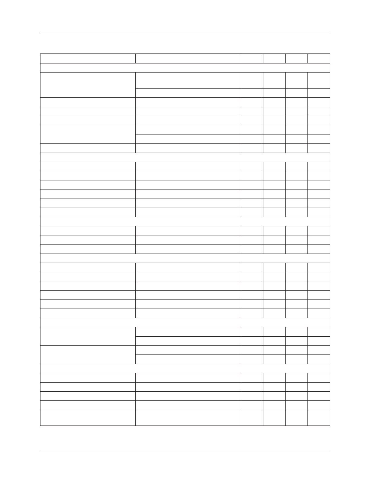
Electrical Specifications
Recommended operating conditions, unless otherwise noted.
Parameter Conditions Min. Typ. Max. Units
DDR, EN Inputs
Input High 2 V
Input Low 0.8 V
FPWM Inputs
FPWM Low 0.1 V
FPWM High FPWM connected to output 0.9 V
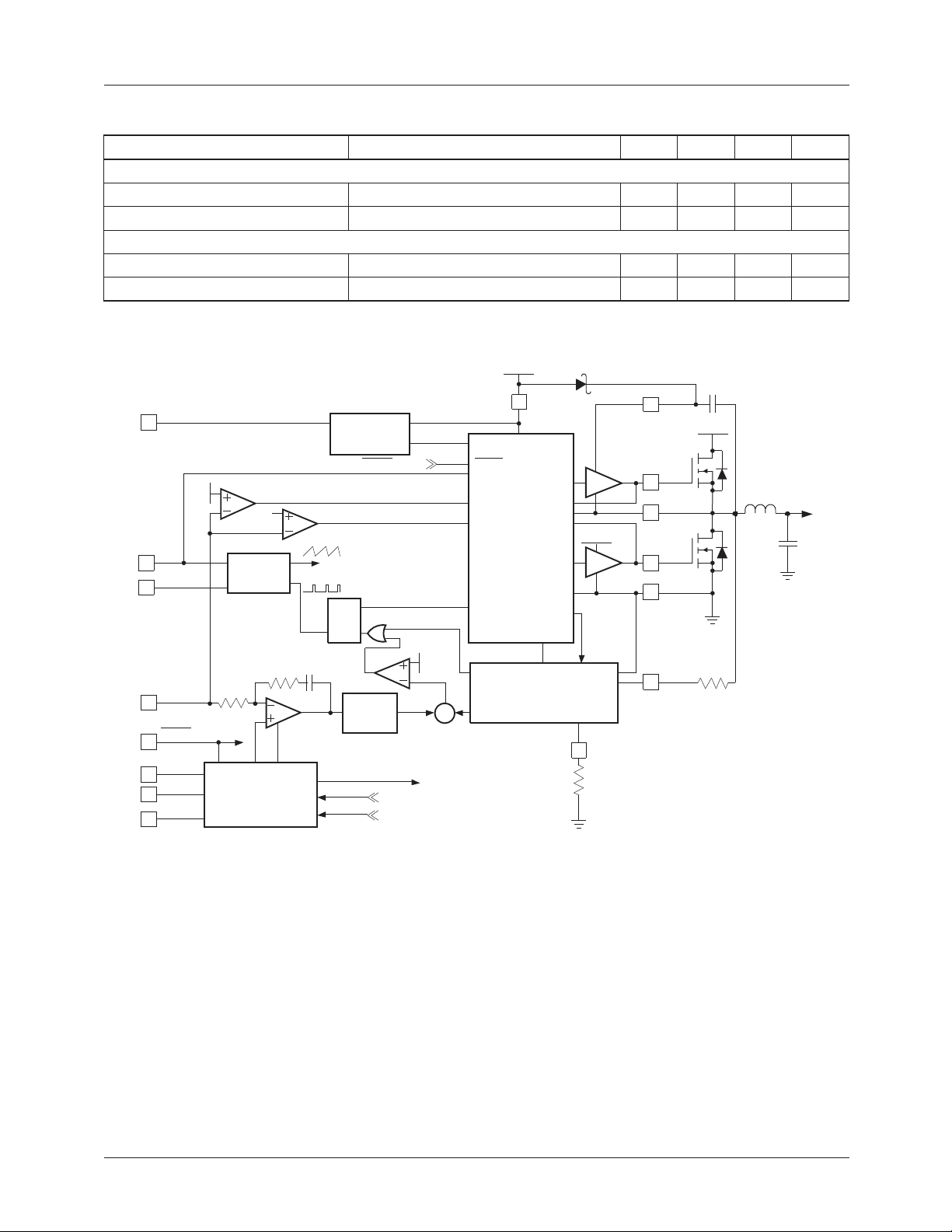
5V
EN
SS
DDR
VIN
VSEN
FPWM/VOU
SS
GOOD
P
REF2
HYST
OSC
T
Reference and
Soft Start
CL
VDD
POR/UVLO
FPWM/VOU
OVP
RAMP
K
Q
SR
VREF
DUTY
CYCLE
CLAMP
EA
PWM
PWM /HYS
DD
T
RAMP
T
R
FPWM
DDR
HYST
ADAPTIVE
GATE
CONTROL LOGIC
PWM
PWM /HYST
ILIM det.
CURRENT PROCESSING
I
Σ
OUT
MODE
S/H
VDD
R
ILIM
ILIM
BOOT
HDRV
SW
LDRV
PGND
ISNS
Q1
Q2
R
VIN
SENSE
C
BOOT
L
(continued)
VOUT
OUT
C
OUT
Figure 3. IC Block Diagram
6
REV. 1.1.7 4/4/03
 Loading...