

Fairchild Semiconductor FAN5235 Datasheet
www.fairchildsemi.com
FAN5235
System Electronics Regulator for Mobile PCs
Features
• Synchronous rectification
• ±1% precision internal reference
• >90% efficiency
• Input and output voltage feedback
• 5.4V to 24V input voltage range
• Internally set 300kHz ±15% oscillator
• 5V and 3.3V Main outputs switch out of phase
• 5V-ALWAYS and 3.3V-ALWAYS outputs
• Adjustable boost converter for 12V
• Boost converter slaved to 5V Main
• Input UVLO
• Outputs OVP of Buck Converters
• Precision current limit option for 5V, 3.3V Main
• Power Good Voltage Monitor
Applications
• Notebook PCs and PDAs
• Hand-held portable instruments
Description
The FAN5235 is a high efficiency and high precision
DC/DC controller for notebook converters. Utilization of
both input and output voltage feedback in a current-mode
control allows for fast and stable loop response over a wide
range of input and output voltage variations. The two main
regulators switch out of phase to minimize input ripple
current.
Current sense based on MOSFET Rdson gives maximum
efficiency, while also permitting use of a sense resistor for
high accuracy. An externally adjustable boost converter can
be set to generate 12V.
The F AN5235 is av ailable in a 24-pin QSOP package, and in
a 24-pin TSSOP package.
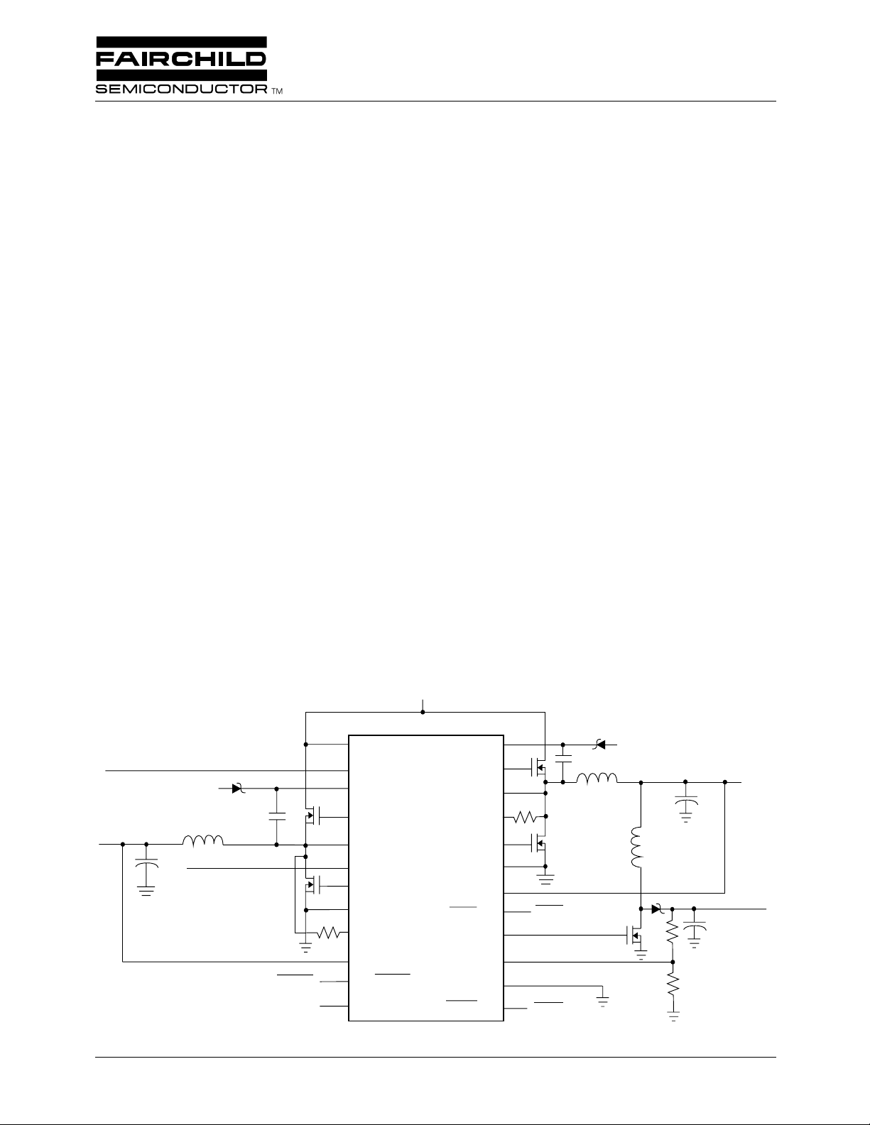
Typical Application
3.3V-ALWAYS@50mA
5V-ALWAYS
3.3V @ 5A
+
5V-ALWAYS@ 50mA
SDN3.3
PGOOD
Vin = 5.4-24V
FAN5235
1 VIN
2 3.3 ALW
3 CPUMP3.3
4 HSD3.3
5 SW3.3
6 5V-ALW
7 LSD3.3
8 GND3.3
9 ISEN3.3
10 VFB3.3
11 SDN3.3
12 PGOOD
CPUMP5 24
HSD5 23
SW5 22
ISEN5 21
LSD5 20
GND5 19
VFB5 18
SDN5 17
SW12 16
VFB12 15
SGND 14
SDWN 13
SDN5
VFB12
SDWN
5V-ALWAYS
5V @ 5A
+
12V @ 120mA
+
REV. 1.3.3 1/3/02
2
FAN5235
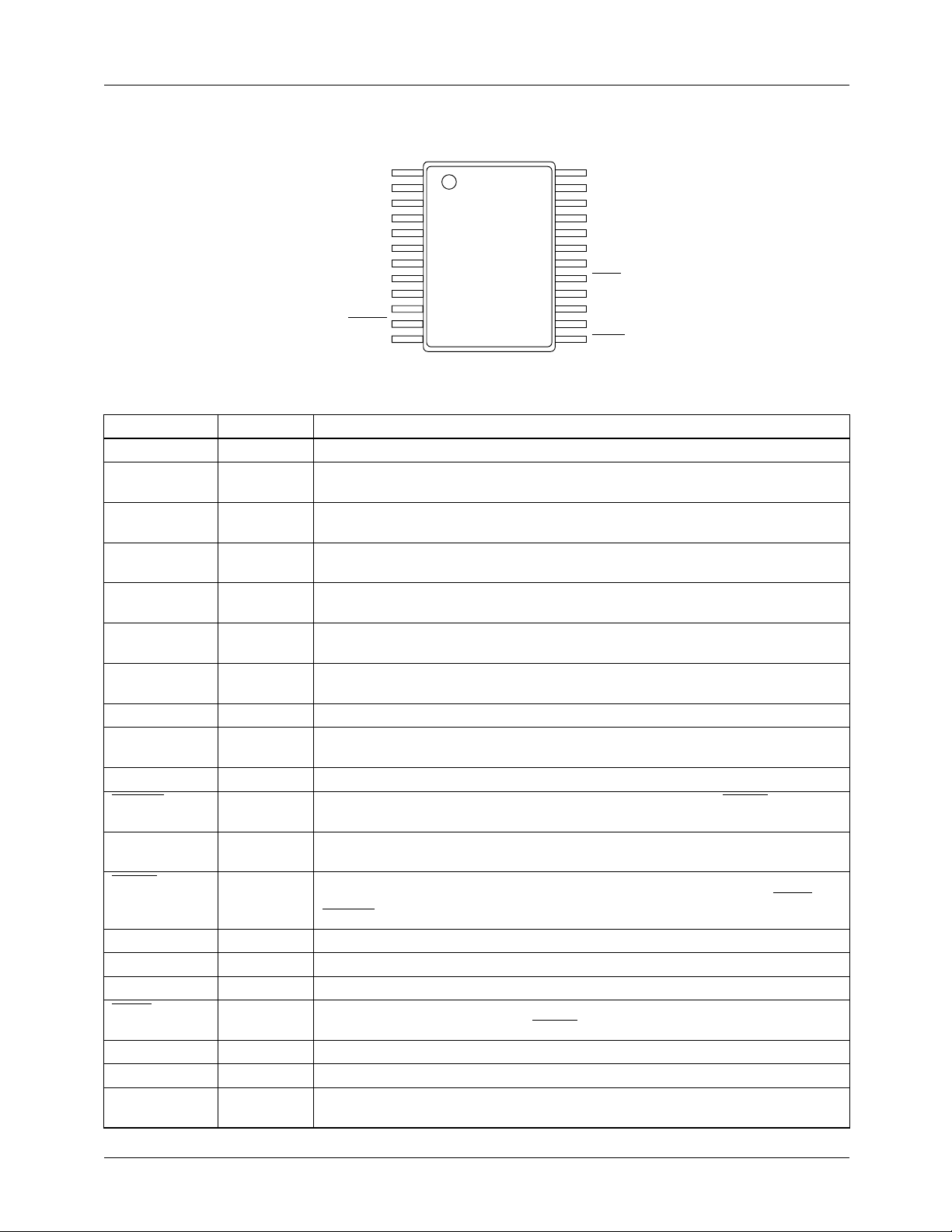
Pin Assignments
3.3V-ALWA YS
VIN
CPUMP3.3
HSD3.3
SW3.3
5V-ALWA YS
LSD3.3
GND3.3
ISEN3.3
VFB3.3
SDN3.3
PGOOD
Pin Description
Pin Name Pin Number Pin Function Description
VIN 1
3.3V-ALWAYS 2
CPUMP3.3 3
HSD3.3 4
SW3.3 5
5V-ALWAYS 6
LSD3.3 7
GND3.3 8
ISEN3.3 9
VFB3.3 10
SDN3.3
PGOOD 12
SDWN
SGND 14
VFB12 15
SW12 16
SDN5
VFB5 18
GND5 19
LSD5 20
11
13
17
Input power.
3.3V Always on linear regulator. Load current on pins 2 and 6 must not exceed
50mA total.
Charge Pump 3.3V. High side Gate drive voltage for 3.3V. This pin is to be
connected to SW3.3 through a 100nF cap. and to 5V-ALWAYS through a diode
High-side gate driver for 3.3V. Connect this pin directly to the gate of an
N-channel MOSFET. The trace from this pin to the MOSFET gate should be < 1".
High side FET Source and Low Side FET Drain Switching Node. Switching
node for 3.3V.
5V Always on linear regulator output. The sum of the load currents on pins 2
and 6 must not exceed 50mA total.
Low-side gate driver for 3.3V. Connect this pin directly to the gate of an
N-channel MOSFET. The trace from this pin to the MOSFET gate should be < 1".
Ground for 3.3V MOSFET.
Current sense for 3.3V. This pin should be connected to the Drain of the bottom
Mosfet with an appropriate resistor and an RC filter. See Application Section.
Voltage feedback for 3.3V.
Soft Start and ON/OFF for 3.3V. OFF=GND. ON=open with SDWN=High. Use
open collector device for control.
Power Good Flag. An open collector output that will be logic low if any output
voltage is not above 89% of the nominal output voltage.
Master Shutdown. Shutdown for all power. Off when low. When high
5V/3.3V-ALWAYS are ON while 5V/3.3V-Main are ready to turn on if SDN5,
SDN3.3 go open.
Signal ground.
Voltage feedback for 12V.
FET driver for 12V Boost.
Enable/Soft Start for 5V and 12V. Soft start and ON/OFF for 5V & 12V.
OFF=Grounded. ON=open with SDWN
Voltage feedback for 5V.
Ground for 5V MOSFET.
Low side FET driver for 5V. Connect this pin directly to the gate of an N-channel
MOSFET. The trace from this pin to the MOSFET gate should be < 1".
1
2
3
4
5
6
7
8
9
10
11
12
T op Vie w
24
23
22
21
20
19
18
17
16
15
14
13
CPUMP5
HSD5
SW5
ISEN5
LSD5
GND5
VFB5
SDN5
SW12
VFB12
SGND
SDWN
=High.
REV. 1.3.3 1/3/02
FAN5235
Pin Description
Pin Name Pin Number Pin Function Description
ISEN5 21
SW5 22
HSD5 23
CPUMP5 24
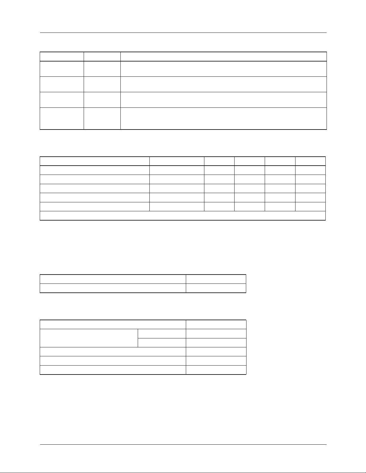
Absolute Maximum Ratings
V
IN
SW, ISEN Pins,SDWN Pin -0.3 27 V
CPUMP, HSD Pins -0.3 33 V
SDN, VFB, V_always pins -0.3 6.5 V
CPUMP to SW pins, and all other pins -0.3 6.5 V
The sum of the load currents on pins 2 and 6 must not exceed 60mA total
Note:
1. Stresses beyond "Absolute Maximum Ratings" may cause permanent device damage. Continuous exposure to absolute
maximum rating conditions may affect device reliability. Functional operation of the device at these or any other conditions
beyond those indicated in the operational sections of the specification is not implied.
(Continued)
Current Sense for 5V. This pin should be connected to the drain of the bottom
Mosfet using appropriate resistor and RC filter. See Application Section.
High Side Driver Source and Low Side Driver Drain Switching Node.
Switching node for 5V.
High side FET driver for 5V. Connect this pin directly to the gate of an N-channel
MOSFET. The trace from this pin to the MOSFET gate should be < 1".
Charge Pump 5V. High side Gate drive voltage for 5V. High side Gate drive
voltage for 5V. This pin is to be connected to SW5 through a 100nF cap. and to
5V-ALWAYS through a diode.
1
Parameter Conditions Min. Typ. Max. Units
-0.3 27 V
Recommended Operating Conditions
Input Voltage, V
Ambient Temperature, T
IN
A
+5.4V to 24V
-20°C to 85°C
Thermal Information
Thermal Resistance, θ
Thermal Resistance, θ
Maximum Junction Temperature 150°C
Storage Temperature Range -65°C to 150°C
Maximum Lead Temperature, Soldering 10 Sec 300°C
88°C/W
JA
QSOP 28.5°C/W
JC
TSSOP 16°C/W
REV. 1.3.3 1/3/02
3
4
Ω
Ω
Ω
Ω
FAN5235
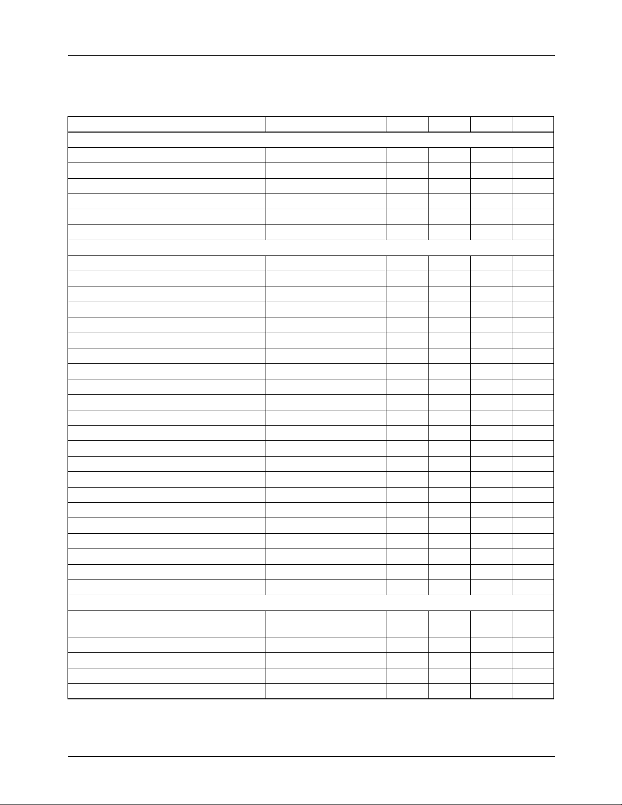
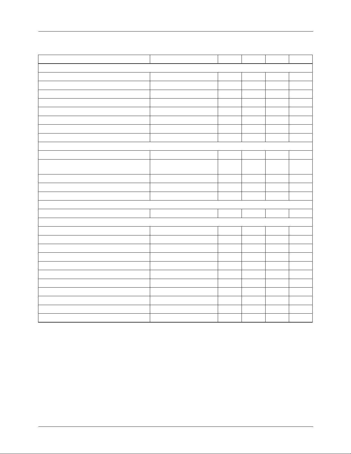
ELECTRICAL SPECIFICATIONS
Operating Conditions
Recommended Operating Conditions Unless Noted Refers to Block Diagrams
Parameter Conditions Min. Typ. Max. Units
Supply
V
Input Supply Voltage (DC loading only) Note 1 5.4 24 V
IN
Input Quiescent Current H/LSD Open 1.4 3 mA
Stand-by 300 400 µA
Shut-down <1 5 µA
Input UVLO Threshold Rising Vbat 4.3 4.7 5.1 V
hysteresis 500 mV
5V and 3.3V Main Regulators
Output Voltage Precision 0.1 to 5.5A, 5.4 to 24V -2 +2 %
Oscillator Frequency, f
osc
HSD On-Resistance, pull up 7 12
HSD On Resistance pull down 4 10
LSD On-Resistance, pull up 6 9
LSD On Resistance pull down 5 8
HSD On Output, V
HSD Off Output, V
LSD On Output, V
LSD Off Output, V
CPUMP
GS
5V-Always
GS
-V
-V
GS
GS
I = 10µA 100 mV
I = 10µA 100 mV
I = 10µA 100 mV
I = 10µA 100 mV
Ramp Amplitude, pk-pk VIN = 16V 2 V
Ramp Offset 0.5 V
Ramp Gain from V
IN
Error Amplifier GBW 3 MHz
Current Limit Threshold R2, R8 = 1K Ω
Over Voltage Threshold 2µs delay 110 115 120 %VO
Under Voltage Threshold 2µs delay 70 75 80 %VO
SDN/SS Full On Voltage Min. (End of Soft Start) 4.2 V
SDN/SS Full Off Voltage Max. 800 mV
Max Duty Cycle 94 %
Min PWM Time 200 nsec
VFB3.3 Input Leakage Current 40 55 70 µA
12V Regulator
Output Voltage Precision V_5 =4.9 to 5.1V
and Io=0 to 150mA
V
FB12
V
Input Current Note 2 100 200 nA
FB12
Oscillator Frequency (f
/3) 85 100 115 kHz
osc
Gate Drive On-Resistance High or Low 6 12
255 300 345 kHz
125 mV/V
90 135 180 µA
-2 +2 %
2.472 V
Ω
REV. 1.3.3 1/3/02
Ω
FAN5235
Operating Conditions
(Continued)
Recommended Operating Conditions Unless Noted Refers to Block Diagrams
Parameter Conditions Min. Typ. Max. Units
12V Regulator (Continued)
On Output, V
Off Output, V
5V-Always
GS
-V
GS
I = 10µA 100 mV
I = 10µA 100 mV
Ramp Amplitude, pk-pk 2 V
Error Amplifier GBW 1 MHz
Under Voltage Shut Down 2µs delay 70 76 80 %V
Over Voltage Shut Down Measured at VFB
12
115 %V
O
O
Min Duty Cycle 0 %
Max Duty Cycle (By design) 32 33 34 %
5V and 3.3V Always
Bypass Switch rdson 1.3 1.5
Linear Regulator Accuracy 5.6 to 24V, 0 to 50mA,
-3.3 2 %
5V Main On or Off
Rated Output Current I
3.3
+ I
5
050mA
Over-current Limit 2µs delay 100 180 mA
Under-voltage Threshold 2µs delay 70 75 80 %
Reference
Internal Reference Accuracy 0-70°C -1 1 %
Control Functions
SDWN Off Voltage Max. 800 mV
SDWN On Voltage Min. 3 V
Over-temperature Shutdown, t
j
150 °C
Over-temperature Hysteresis 25 °C
PGOOD Threshold PWM Buck Converters -14 -11 -8.5 %V
1
O
PGOOD Sink Current -4 mA
PGOOD leakage 1µA
+5V Analog Softstart Css=100nF 65 msec
+3.3V Analog Softstart Css=100nF 65 msec
Soft Start Current 5 µA
PGOOD Min Pulse Width Note 2 5 10 µs
Notes
1. The minimum input voltage does not include voltage drop in the source supply due to source resistance. It is operating voltage
for static load conditions. To get acceptable load transient performance, the input voltage required will be much higher, in the
7.5 to 8.5 volt range or even higher depending on the severity of dynamic load, source impedance and input and output
capacitance and inductor values. The user should thoroughly test the performance at minimum input voltage using intended
component values and transient loading.
2. Min/Max specifications are guaranteed by design.
REV. 1.3.3 1/3/02
5
 Loading...