

Fairchild Semiconductor DM74ALS02SJX, DM74ALS02SJ, DM74ALS02N, DM74ALS02MX, DM74ALS02M Datasheet
© 2000 Fairchild Semiconductor Corporation DS006175 www.fairchildsemi.com
September 1986
Revised February 2000
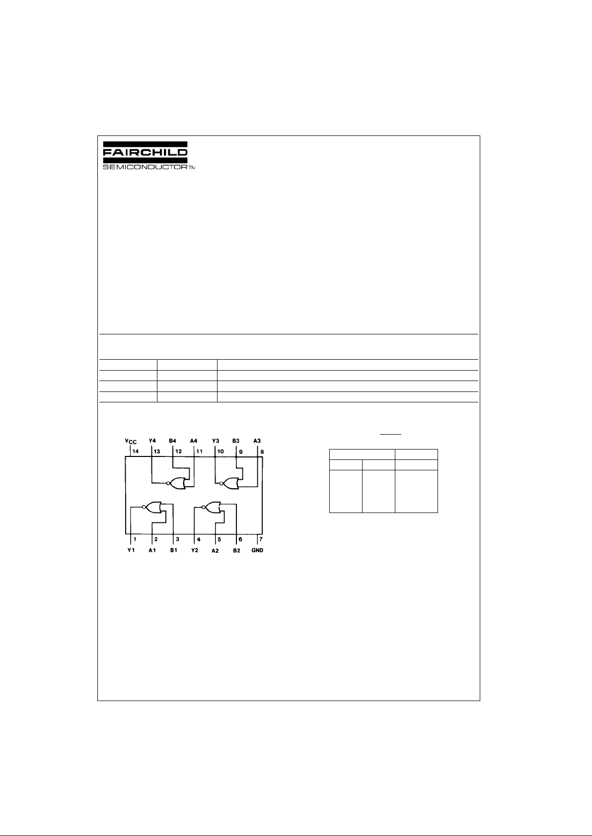
DM74ALS02 Quad 2-Input NOR Gate
DM74ALS02
Quad 2-Input NOR Gate
General Description
This device contains four independent gates, each of which
performs the logic NOR function.
Features
■ Switching specifications at 50 pF
■ Switching specifications guaranteed over full tempera-
ture and V
CC
range
■ Advanced oxide-isolated, ion-implanted Schottky TTL
process
■ Functionally and pin for pin compatible with Schottky
and low power Schottky TTL counterpart
■ Improved AC performance over Schottky and low power
Schottky counterparts
Ordering Code:
Devices also availab le in Tape and Reel. Specify by appending th e s uffix let t er “X” to the ordering code.
Connection Diagram Function Table
H = HIGH Logic Level
L = LOW Logic Level
Order Number Package Number Package Description
DM74ALS02M M14A 14-Lead Small Outline Integrated Circuit (SOIC), JEDEC MS-012, 0.150 Narrow
DM74ALS02SJ M14D 14-Lead Small Outline Package (SOP), EIAJ TYPE II, 5.3mm Wide
DM74ALS02N N14A 14-Lead Plastic Dual-In-Line Package (PDIP), JEDEC MS-001, 0.300 Wide
Y = A + B
Inputs Output
AB Y
LL H
LH L
HL L
HH L
www.fairchildsemi.com 2
DM74ALS02
Absolute Maximum Ratings(Note 1)
Note 1: The “Absolute Maximum Ratin gs” are those v alues beyon d which
the safety of the dev ice cannot be guaranteed. T he device sh ould not be
operated at these limits. The parametric values defined in the Electrical
Characteristics tables are not guaranteed at the absolute maximum ratings.
The “Recommend ed O peratin g Cond itions” t able w ill defin e the co ndition s
for actual device operation.
Recommended Operating Conditions
Electrical Characteristics
over recommended operating free air temperature range. All typical values are measured at VCC = 5V, TA = 25°C.
Switching Characteristics
over recommended operating free air temperature range.
Supply Voltage 7V
Input Voltage 7V
Operating Free Air Temperature Range 0°C to +70°C
Storage Temperature Range −65°C to +150°C
Typical θ
JA
N Package 86.5°C/W
M Package 116.0°C/W
Symbol Parameter Min Nom M ax Units
V
CC
Supply Voltage 4.5 5 5.5 V
V
IH
HIGH Level Input Voltage 2 V
V
IL
LOW Level Input Voltage 0.8 V
I
OH
HIGH Level Output Current −0.4 mA
I
OL
LOW Level Output Current 8 mA
T
A
Free Air Operating Temperature 0 70 °C
Symbol Parameter Conditions Min Typ Max Units
V
IK
Input Clamp Voltage VCC = 4.5V, II = −18 mA −1.5 V
V
OH
HIGH Level IOH = −0.4 mA
VCC − 2V
Output Voltage VCC = 4.5V to 5.5V
V
OL
LOW Level
VCC = 4.5V IOL = 8 mA 0.35 0.5 V
Output Voltage
I
I
Input Current @ Max.
VCC = 5.5V, VIH = 7V 0.1 mA
Input Voltage
I
IH
HIGH Level Input Current VCC = 5.5V, VIH = 2.7V 20 µA
I
IL
LOW Level Input Current VCC = 5.5V, VIL = 0.4V −0.1 mA
I
O
Output Drive Current VCC = 5.5V VO = 2.25V −30 −112 mA
I
CC
Supply Current VCC = 5.5V Outputs HIGH 0.85 2.2 mA
Outputs LOW 2.16 4 mA
Symbol Parameter Conditions Min Max Units
t
PLH
Propagation Delay Time VCC = 4.5V to 5.5V
312ns
LOW-to-HIGH Level Output RL = 500Ω
t
PHL
Propagation Delay Time CL = 50 pF
3 10 ns
HIGH-to-LOW Level Output
 Loading...