

Fairchild Semiconductor DM7474N, DM7474M Datasheet
September 1986
Revised February 2000
DM7474
Dual Positive-Edge-Triggered D-Type Flip-Flops with
Preset, Clear and Complementary Outputs
DM7474 Dual Positive-Edge-Triggered D-Type Flip-Flops with Pres et, Clear and Complementary Outputs
General Description
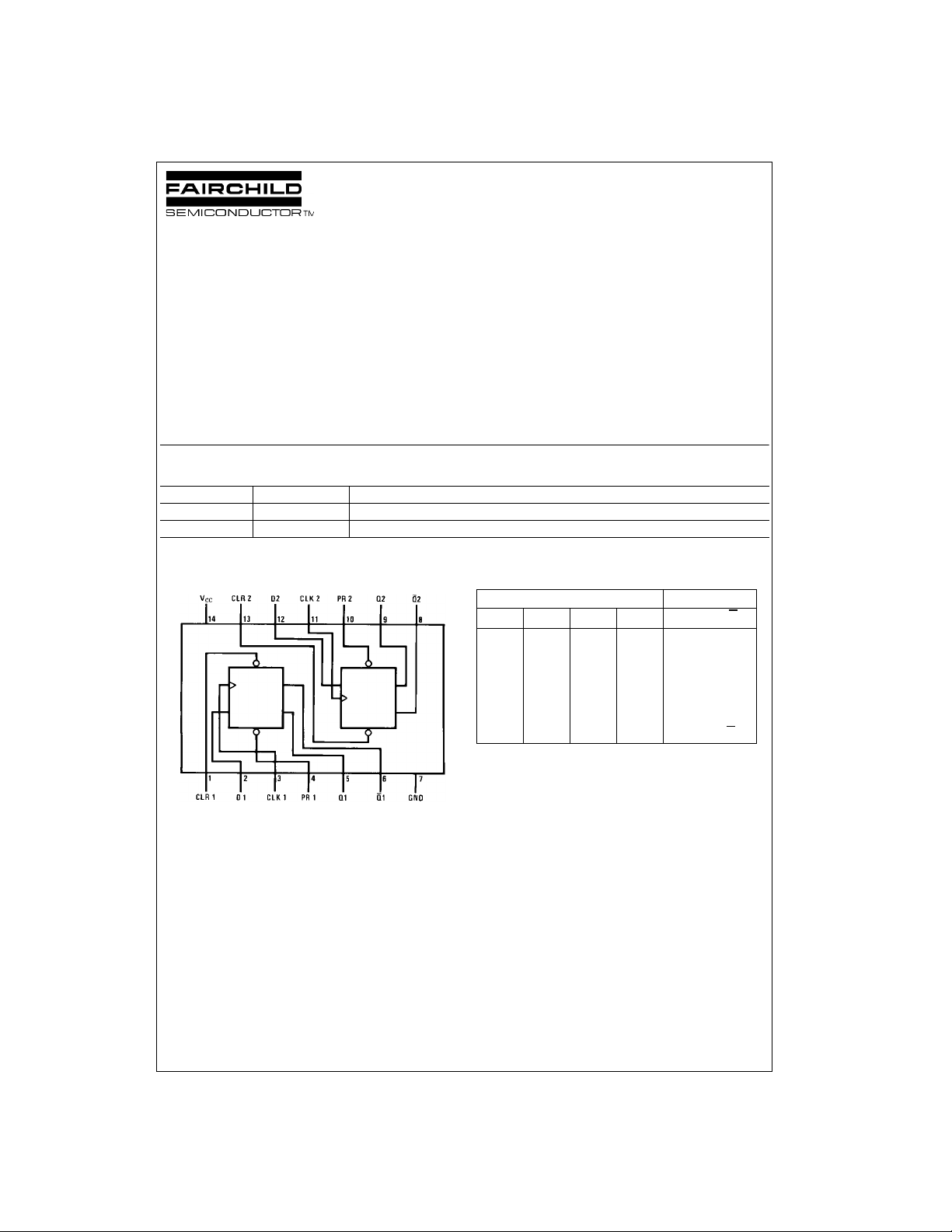
This device contains two independent positive-edge-triggered D-type flip-flops with complementary outputs. The
information on the D i nput is accepted by the flip-flops on
the positive going edge of the clock pulse. The triggering
occurs at a voltage level and is not directly r elated to the
transition time of the rising ed ge of the clock. The data on
the D input may be changed wh ile the clock is LOW or
HIGH without affecting the outputs as long as the data
setup and hold times are not violated. A LOW logic level on
the preset or clear inputs will set or reset the outputs
regardless of the logic levels of the other inputs.
Ordering Code:
Order Number Package Number Package Description
DM7474M M14A 14-Lead Small Outline Integrated Circuit (SOIC), JEDEC MS-012, 0.150 Narrow
DM7474N N14A 14-Lead Plastic Dual-In-Line Package (PDIP), JEDEC MS-001, 0.300 Wide
Devices also availab le in Tape and Reel. Specify by appending th e s uffix let t er “X” to the ordering cod e.
Connection Diagram Function Table
Inputs Outputs
PR CLR CLK D Q Q
LHXXHL
HLXXLH
LLXXH
HH↑ HHL
HH↑ LLH
HHLXQ
H = HIGH Logic Level
X = Either LOW or HIGH Logic Level
L = LOW Logic Level
↑ = Positive-going transit ion of the clock.
= The out put logic lev el of Q be fore the in dica ted input con ditio ns were
Q
0
established.
Note 1: This configuration is nonstable; that is, it will not persist when either
the preset and/or clear inputs return to thei r inactive (HIGH) level.
(Note 1)H(Note 1)
0
Q
0
© 2000 Fairchild Semiconductor Corporation DS006526 www.fairchildsemi.com
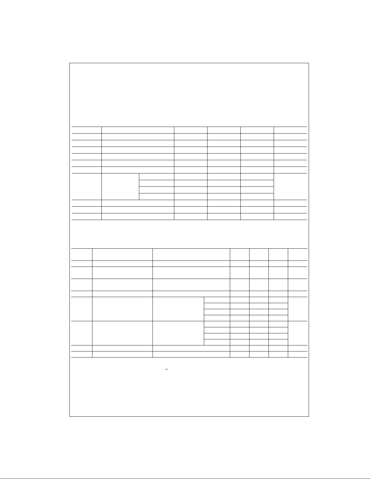
Absolute Maximum Ratings(Note 2)
Supply Voltage 7V
DM7474
Input Voltage 5.5V
Operating Free Air Temperature Range 0°C to +70°C
Storage Temperature Range −65°C to +150°C
Note 2: The “Absolute Maximum Ratin gs” are those v alues beyon d which
the safety of the dev ice cannot be guaranteed. T he device sh ould not be
operated at these limits. The parametric values defined in the Electrical
Characteristics tables are not guaranteed at the absolute maximum ratings.
The “Recommend ed O peratin g Cond itions” t able w ill defin e the c ondit ions
for actual device operation.
Recommended Operating Conditions
Symbol Parameter Min Nom Max Units
V
V
V
I
I
f
t
CC
IH
IL
OH
OL
CLK
W
Supply Voltage 4.75 5 5.25 V
HIGH Level Input Voltage 2 V
LOW Level Input Voltage 0.8 V
HIGH Level Output Current −0.4 mA
LOW Level Output Current 16 mA
Clock Frequency (Note 4) 0 15 MHz
Pulse Width Clock HIGH 30
(Note 4) Clock LOW 37
Clear LOW 30
Preset LOW 30
t
SU
t
H
T
A
Note 3: The symbol (↑) indicates the rising edge of the clock pulse is used for reference.
Note 4: T
Input Setup Time (Note 3)(Note 4) 20↑ ns
Input Hold Time (Note 3)(Note 4) 5↑ ns
Free Air Operating Temperature 0 70 °C
= 25°C and VCC = 5V.
A
Electrical Characteristics
over recommended operating free air temperature range (unless otherwise noted)
Symbol Parameter Conditions Min
V
I
V
OH
V
OL
I
I
I
IH
I
IL
I
OS
I
CC
Note 5: All typicals are at VCC = 5V, TA = 25°C.
Note 6: Not more than one output should be shorted at a time.
Note 7: With all outputs open, I
Note 8: Clear is tested with preset HIGH and preset is tested with clear HIGH.
Input Clamp Voltage VCC = Min, II = −12 mA −1.5 V
HIGH Level VCC = Min, IOH = Max
Output Voltage VIL = Max, VIH = Min
LOW Level VCC = Min, IOL = Max
Output Voltage VIH = Min, VIL = Max
Input Current @ Max Input Voltage VCC = Max, VI = 5.5V 1 mA
HIGH Level VCC = Max D 40
Input Current VI = 2.4V Clock 80
LOW Level VCC = Max D −1.6
Input Current VI = 0.4V Clock −3.2
(Note 8) Clear −3.2
Short Circuit Output Current VCC = Max (Note 6) −18 −55 mA
Supply Current VCC = Max (Note 7) 17 30 mA
is measured with the Q and Q outputs HIGH in tur n. At th e t im e of measurement the c loc k is grounded.
CC
Clear 120
Preset 40
Preset −1.6
2.4 3.4 V
Typ
(Note 5)
0.2 0.4 V
ns
Max Units
µA
mA
www.fairchildsemi.com 2
 Loading...