Fairchild Semiconductor DM7447AN, DM7446AN Datasheet

DM7446A, DM7447A
BCD to 7-Segment Decoders/Drivers
DM7446A, DM7447A BCD to 7-Segment Decoders/Drivers
September 1986
Revised February 2000
General Description
The DM7446A and DM74 47A feature active- LOW outputs
designed for driving common- ano de LEDs or inc and esce nt
indicators directly. All of the circuits have full ripple-blanking input/output controls and a lamp test input. Segment
identification and resu ltant di splays a re shown on a fo llowing page. Display patterns for BCD input counts above nine
are unique symbols to authenticate input conditions.
All of the circuits incorporate automatic leading and/or trailing-edge, zero-blankin g control (RBI and RBO). Lam p test
(LT) of these devices may be performed at any time when
the BI/RBO node is at a HIGH logic level. All typ es cont ain
an overriding blanking input (BI) which can be used to control the lamp intensity (by pulsing) or to inhibit the outputs.
Features
■ All circuit types featur e lamp inte nsity modulati on capability
■ Open-collector outputs drive indicators directly
■ Lamp-test provision
■ Leading/trailing zero suppression
Ordering Code:
Order Number Package Number Package Description
DM7446AN N16E 16-Lead Plastic Dual-In-Line Package (PDIP), JEDEC MS-001, 0.300 Wide
DM7446AN N16E 16-Lead Plastic Dual-In-Line Package (PDIP), JEDEC MS-001, 0.300 Wide
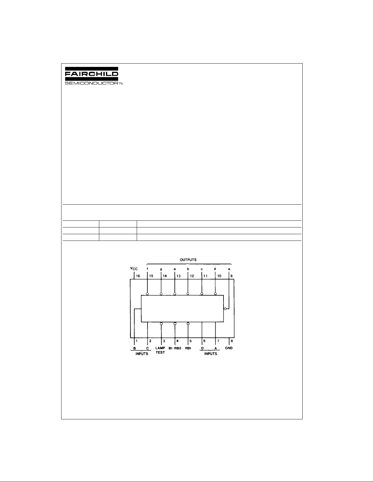
Connection Diagram
© 2000 Fairchild Semiconductor Corporation DS006518 www.fairchildsemi.com

Function Table
Decimal or Inputs BI/RBO Outputs
Function LT RBI D C B A (Note 1) a b c d e f g
0 HHLLLL H LLLLLLH
1 HXLLLH H HLLHHHH
2 HXLLHL H LLHLLHL
3 HXLLHH H LLLLHHL
DM7446A, DM7447A
4 HXLHLL H HLLHHLL
5 HXLHLH H LHLLHLL
6 HXLHHL H HHLLLLL
7 HXLHHH H L LLHHHH(Note 2)
8 HXHLLL H LLLLLLL
9 HXHLLH H LLLHHLL
10 HXHLHL H HHHLLHL
11 HXHLHH H HHLL HHL
12 HXHHL L H HLHHHL L
13 HXHHLH H LHHLHLL
14 HXHHHL H HHHLLLL
15 HXHHHH H HHHHHHH
BI XXXXXX L HHHHHHH(Note 3)
RBI HLL LLL L HHHHHHH(Note 4)
LT LXXXXX H LLLLLLL(Note 5)
H = HIGH level, L = LOW level, X = Don’t Care
Note 1: BI/RBO is a wire-AND logic servin g as blanking input (BI) and / or ripple-blanking outp ut ( R BO).
Note 2: The blanking input (BI) must be OPEN o r held at a HIGH logic le v el w hen output functions 0 t hrough 15 are desir ed. The ripple-blanking input (RBI)
must be OPEN or HI GH if blanking of a decimal ze ro is not desired.
Note 3: When a LOW logic level is applied dire c t ly to the blanking input (BI), all segment outputs are HIGH regardless of the level of any other input.
Note 4: When ripple-blanking input (RBI) and inputs A, B, C , and D are at a LOW level with the lamp test input HI GH , all segment outputs go H and the rip-
ple-blanking output (RBO) goes to a LOW level (response condition).
Note 5: When the blanking input/ripple-blanking output (BI/RBO) is OPEN or held HIGH and a LOW is applied to the lamp-test input, all segment outputs are
L.
Note
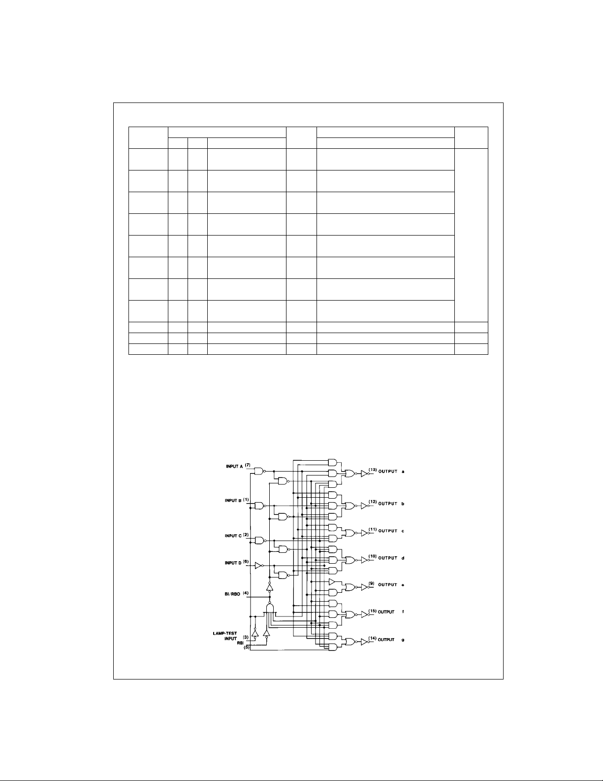
Logic Diagram
www.fairchildsemi.com 2
 Loading...