

Fairchild Semiconductor DM7426N, DM7426CW Datasheet
© 2000 Fairchild Semiconductor Corporation DS006508 www.fairchildsemi.com
August 1986
Revised February 2000
DM7426 Quad 2-Input NAND Gates with High Voltage Open-Collector Outputs
DM7426
Quad 2-Input NAND Gates with
High Voltage Open-Collector Outputs
General Description
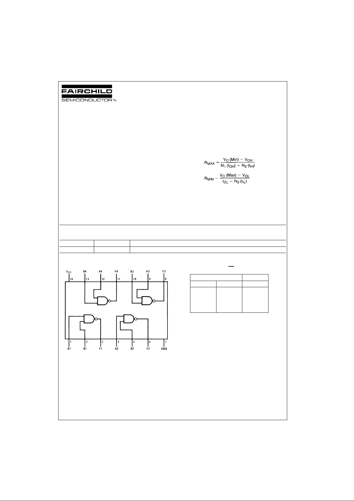
This device contains four independent gates each of which
performs the logic NA ND functio n. The open -collector outputs require external pull-up resistors for proper logical
operation.
Pull-Up Resistor Equations
Where: N1 (IOH) = total maximum output high c urrent
for all outputs tied to pull-up resistor
N
2
(IIH) = total maximum input high current for
all inputs tied to pull-up resistor
N
3
(IIL) = total maximum input low current for
all inputs tied to pull-up resistor
Ordering Code:
Connection Diagram Function Table
Y = AB
H = HIGH Logic Level
L = LOW Logic Level
Order Number Package Number Package Description
DM7426N N14A 14-Lead Plastic Dual-In-Line Package (PDIP), JEDEC MS-001, 0.300 Wide
Inputs Output
ABY
LLH
LHH
HLH
HHL
www.fairchildsemi.com 2
DM7426
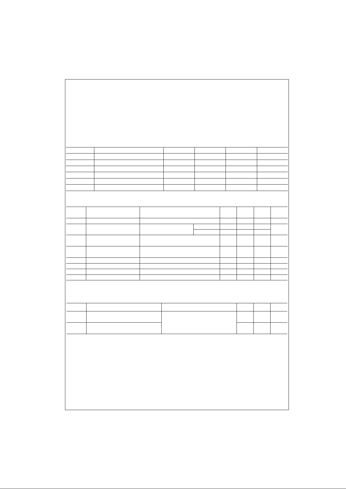
Absolute Maximum Ratings(Note 1)
Note 1: The “Absolute Maximum Ratin gs” are those v alues beyon d which
the safety of the dev ice cannot be guaranteed. T he device sh ould not be
operated at these limits. The parametric values defined in the Electrical
Characteristics tables are not guaranteed at the absolute maximum ratings.
The “Recommend ed O peratin g Cond itions” t able w ill defin e the co ndition s
for actual device operation.
Recommended Operating Conditions
Electrical Characteristics
over recommended operating free air temperature range (unless otherwise noted)
Note 2: All typicals are at VCC = 5V, TA = 25°C.
Switching Characteristics
at VCC = 5V and TA = 25°C
Supply Voltage 7V
Input Voltage 5.5V
Output Voltage 15V
Operating Free Air Temperature Range 0°C to +70°C
Storage Temperature Range −65°C to +150°C
Symbol Parameter Min Nom Max Units
V
CC
Supply Voltage 4.75 5 5.25 V
V
IH
HIGH Level Input Voltage 2 V
V
IL
LOW Level Input Voltage 0.8 V
V
OH
HIGH Level Output Voltage 15 V
I
OL
LOW Level Output Current 16 mA
T
A
Free Air Operating Temperature 0 70 °C
Symbol Parameter Conditions Min
Typ
Max Units
(Note 2)
V
I
Input Clamp Voltage VCC = Min, II = −12 mA −1.5 V
I
CEX
HIGH Level VCC = Min VO = 15V 1000
µA
Output Current VIL = Max VO = 12V 50
V
OL
LOW Level VCC = Min, IOL = Max
0.4 V
Output Voltage VIH = Min
I
I
Input Current @ Max VCC = Max,
1mA
Input Voltage VI = 5.5V
I
IH
High Level Input Current VCC = Max, VI = 2.4V 40 µA
I
IL
Low Level Input Current VCC = Max, VI = 0.4V −1.6 mA
I
CCH
Supply Current with Outputs HIGH VCC = Max 4 8 mA
I
CCL
Supply Current with Outputs LOW VCC = Max 12 22 mA
Symbol Parameter Conditions Min Max Units
t
PLH
Propagation Delay Time CL = 15 pF
24 ns
LOW-to-HIGH Level Output RL = 1 kΩ (t
PLH
)
t
PHL
Propagation Delay Time
17 ns
HIGH-to-LOW Level Output
 Loading...