


Fairchild Semiconductor DM74174N Datasheet
DM74174
Hex/Quad D-Type Flip-Flop with Clear
DM74174 Hex/Quad D-Type Flip-Flop with Clear
September 1986
Revised February 2000
General Description
These positive-edg e trigge re d flip-fl ops ut iliz e TTL ci rcuitry
to implement D-type flip-flop logic. All have a direct clear
input.
Information at the D inputs meeting the setup and hold time
requirements is transfer red to the Q outputs on the positive-going edge of the clock pul se. Clock triggerin g occurs
at a particular voltage level and is not directly related to the
transition time of the pos itive-goin g pulse. When the clock
input is at either the HIGH or LOW level, the D inpu t sig nal
has no effect at the output.
Features
■ Contains six flip-flops with single-rail outputs
■ Buffered clock and direct clear inputs
■ Individual data input to each flip-flop
■ Applications include:
Buffer/storage registers
Shift registers
Pattern generators
■ Typical clock frequency 40 MHz
■ Typical power dissipation per flip-fl op 38 mW
Ordering Code:
Order Number Package Number Package Description
DM74174 N16E 16-Lead Plastic Dual-In-Line Package (PDIP), JEDEC MS-001, 0.300 Wide
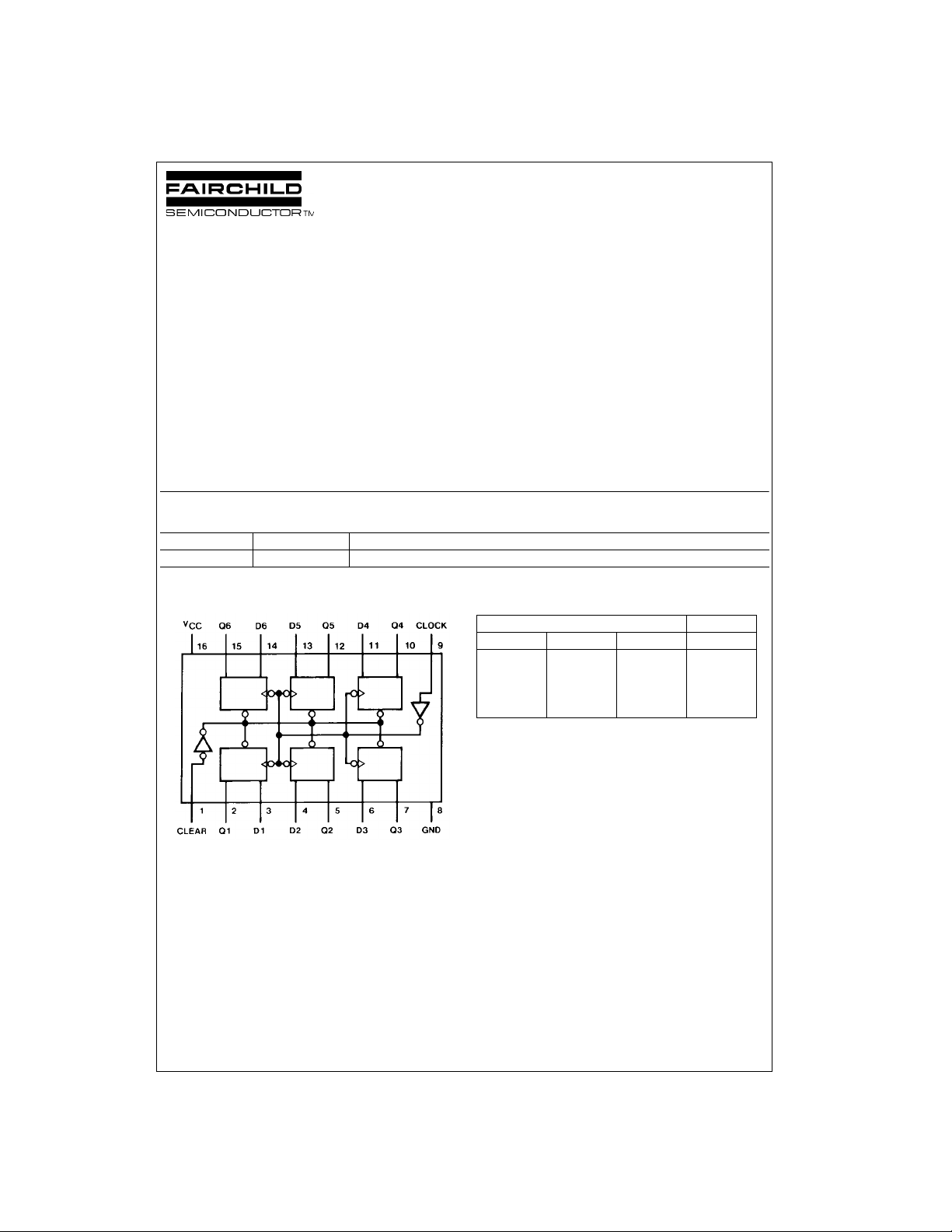
Connection Diagram Function Table
(Each Flip-Flop)
Clear Clock D Q
LXXL
H ↑ HH
H ↑ LL
HLXQ
H = HIGH Level (steady state)
L = LOW Level (steady state)
X = Don’t Care
↑ = Transition from LOW-to-HIGH level
= The level of Q before the indic at ed steady-state inp ut c onditions were
Q
0
established.
Inputs Outputs
0
© 2000 Fairchild Semiconductor Corporation DS006557 www.fairchildsemi.com
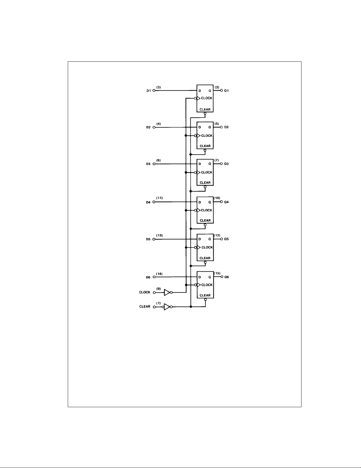
Logic Diagram
DM74174
www.fairchildsemi.com 2