

Fairchild Semiconductor DM74145N Datasheet
DM74145
BCD to Decimal Decoders/Drivers
DM74145 BCD to Decimal Decoders/Drivers
September 1986
Revised February 2000
General Description
These BCD-to-decimal decoders/drivers consist of eight
inverters and ten, four-input NAND gates. The inverters are
connected in pairs to mak e BCD input data available for
decoding by the NAND gates. Fu ll decoding of BCD input
logic ensures that all outputs remain OFF for all invalid
(10–15) binary input conditions. These decoders feature
high-performance, NPN output transistors designed for use
as indicator/relay drivers, or as open-collector logic-circuit
drivers. The high -breakdown output transistors ar e compatible for interfacing with most MOS integrated circuits.
Features
■ Full decoding of input logic
■ 80 mA sink-current capability
■ All outputs are OFF for invalid BCD input conditions
Ordering Code:
Order Number Package Number Package Description
DM74145N N16E 16-Lead Plastic Dual-In-Line Package (PDIP), JEDEC MS-001, 0.300 Wide
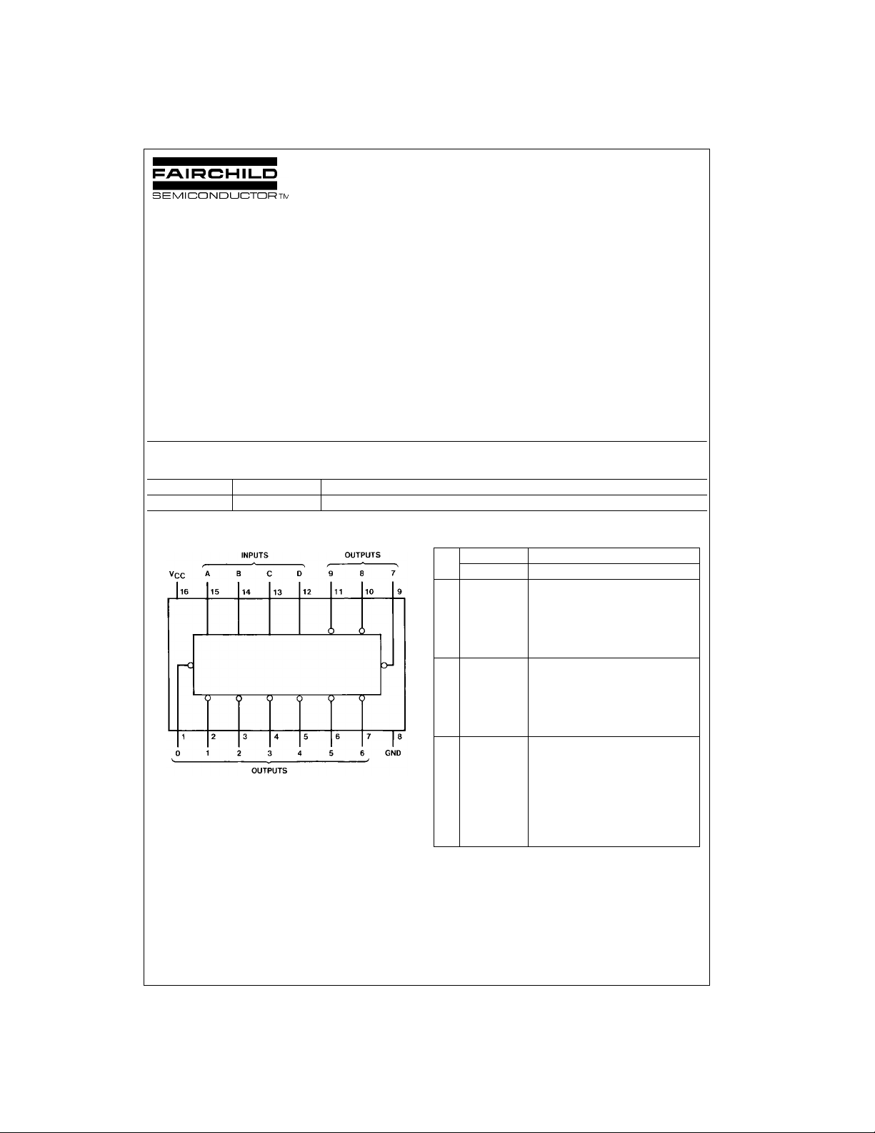
Connection Diagram Function Table
No. Inputs Outputs
DCBA0123456789
0 LLLLLHHHHHHHHH
1 LL LHHLHHHHHHHH
2 LLHLHHLHHHHHHH
3 LLHHHHHLHHHHHH
4 LHL LHHHHLHHHHH
5 LHLHHHHHHLHHHH
6 LHHLHHHHHHLHHH
7 LHHHHHHHHHHLHH
8 HLL LHHHHHHHHLH
9 HLLHHHHHHHHHHL
I HLHLHHHHHHHHHH
N HLHHHHHHHHHHHH
V HHLLHHHHHHHHHH
A HHLHHHHHHHHHHH
L HHHLHHHHHHHHHH
I HHHHHHHHHHHHHH
D
H = HIGH Level (OFF)
L = LOW Level (ON)
© 2000 Fairchild Semiconductor Corporation DS006544 www.fairchildsemi.com
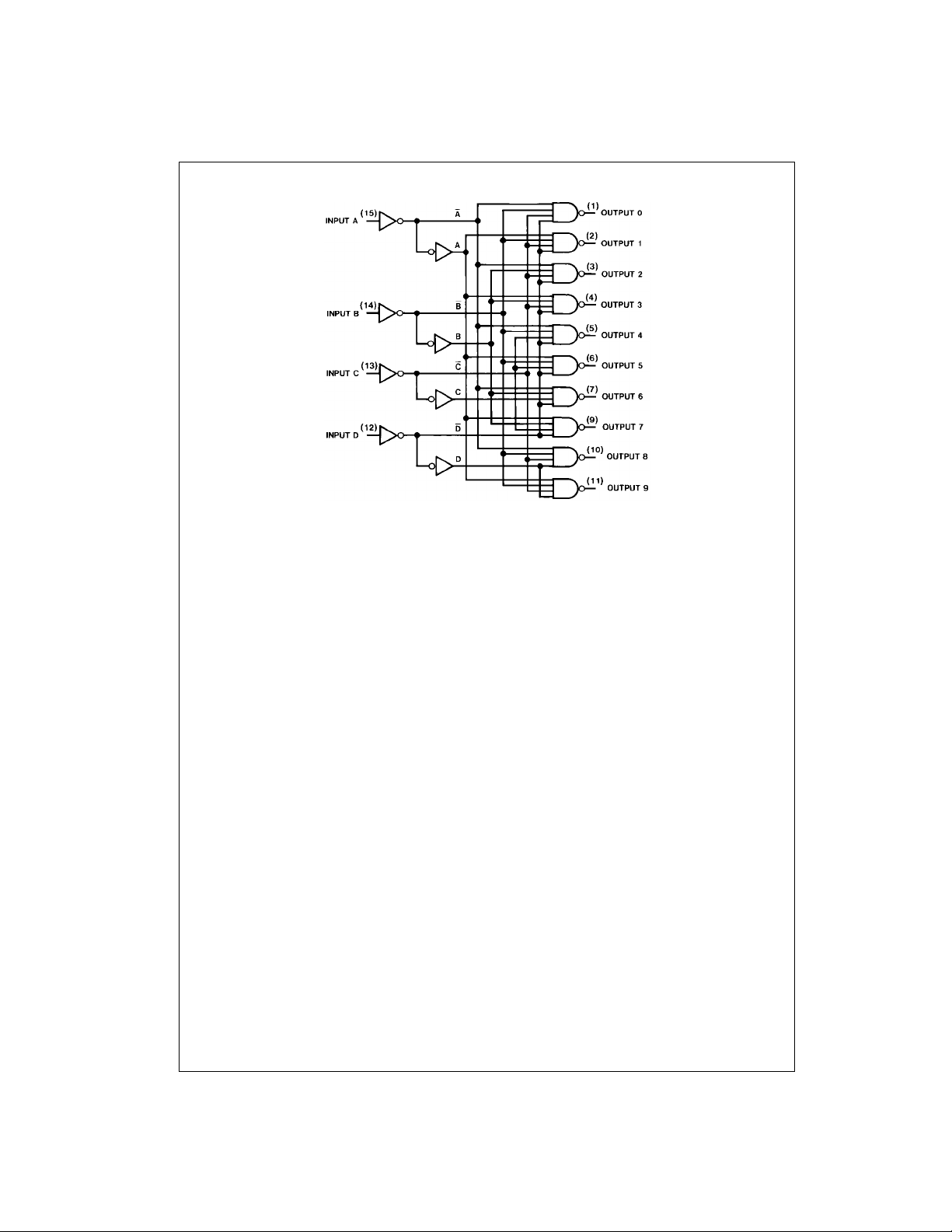
Logic Diagram
DM74145
www.fairchildsemi.com 2
 Loading...