

Fairchild Semiconductor 74VHCT240ASJX, 74VHCT240ASJ, 74VHCT240AN, 74VHCT240AMX, 74VHCT240AMTCX Datasheet
...
March 1997
Revised March 1999
74VHCT240A Octal Buffer/Line Driver with 3-STATE Outputs
© 1999 Fairchild Semiconductor Corporation DS500002.prf www.fairchildsemi.com
74VHCT240A
Octal Buffer/Line Driver with 3-ST ATE Outputs
General Description
The VHCT240A is an advanced high speed CM OS octal
bus transceiver fabricated with silicon gate CM OS techn ology. It achieves high speed operati on similar to equival ent
Bipolar Schottky TTL while maintaining the CMOS low
power dissipation. The VHCT240A is an inverting 3-STATE
buffer having two active-LO W output e nables. This device
is designed to be used as 3-STATE memory address drivers, clock drivers, and bus oriented transmitter/receivers.
Protection circuits ensu re that 0V to 7V can be applied to
the input and output (No te 1) pins without regard to the
supply voltage. These circuits preven t device destruction
due to mismatched supply and i nput/output voltage s. This
device can be used to in terface 5V to 3V system s and tw o
supply systems such as battery back up.
Note 1: Outputs in OFF-State
Features
■ High Speed: tPD = 5.6 ns (typ) at VCC = 5V
■ Power down protection is provided on inputs and
outputs
■ Low power dissipation: I
CC
= 4 µA (max) @ TA = 25°C
■ Pin and function compatible with 74HCT240
Ordering Code:
Surface mount pack ages are also available on Tape and Reel. Specify by appending the s uffix let te r “X” to the ordering code.
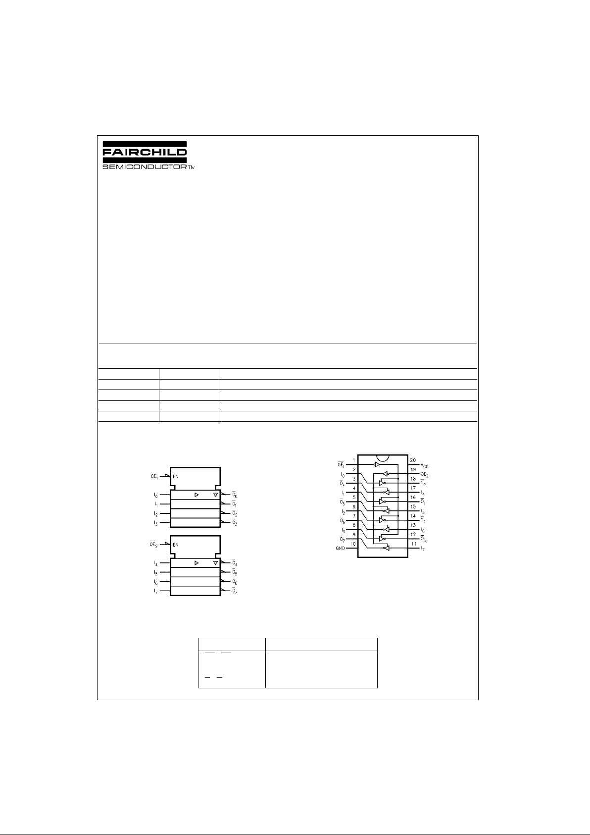
Logic Symbol
IEEE/IEC
Connection Diagram
Pin Descriptions
Order Number Package Number Package Description
74VHCT240AM M20B 20-Lead Small Outline Integrated Circuit (SOIC), JEDEC MS-013, 0.300 Wide
74VHCT240ASJ M20D 20-Lead Small Outline Package (SOP), EIAJ TYPE II, 5.3mm Wide
74VHCT240AMTC MTC20 20-Lead Thin Shrink Small Outline Package (TSSOP), JEDEC MO-153, 4.4mm Wide
74VHCT240AN N20A 20-Lead Plastic Dual-In-Line Package (PDIP), JEDEC MS-001, 0.300 Wide
Pin Names Description
OE
1
, OE
2
3-STATE Output Enable
I
0–I7
Inputs
O
0–O7
Outputs 3-STATE Outputs
www.fairchildsemi.com 2
74VHCT240A
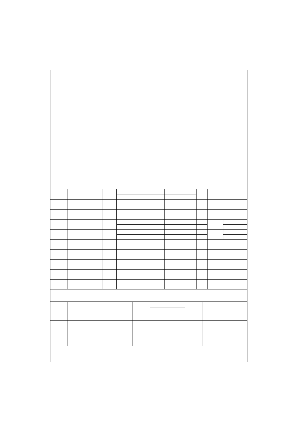
Truth Tables
H - HIGH Voltage Level
L - LOW Voltage Level
X - Immaterial
Z - High Impedance
Inputs Outputs
(Pins 12, 14, 16, 18)
OE
1
I
n
LL H
LH L
HX Z
Inputs Outputs
(Pins 3, 5, 7, 9)
OE
1
I
n
LL H
LH L
HX Z
3 www.fairchildsemi.com
74VHCT240A
Absolute Maximum Ratings(Note 2) Recommended Operating
Conditions
(Note 6)
Note 2: Absolute Maximum Ratings are valu es beyond whic h the device
may be damaged or ha ve its useful life impaire d. The datab ook specifications should be met, without exception, to ensure that the system design is
reliable over its p ower supp ly, temperature, and o utput/input loading variables. Fairchild does not recommend operation outside databook specifications.
Note 3: HIGH or LOW state. I
OUT
absolute maximum rating must be
observed.
Note 4: When outputs are in OFF-S ta t e or w hen V
CC
= OV.
Note 5: V
OUT
< GND, V
OUT
> VCC (Outputs Active).
Note 6: Unused inputs must be held HIGH o r LOW. They may not float.
DC Electrical Characteristics
Noise Characteristics
Note 7: Parameter gu aranteed by design.
Supply Voltage (VCC) −0.5V to +7.0V
DC Input Voltage (V
IN
) −0.5V to +7.0V
DC Output Voltage (V
OUT
)
(Note 3) −0.5V to V
CC
+ 0.5V
(Note 4) −0.5V to +7.0V
Input Diode Current (I
IK
) −20 mA
Output Diode Current (I
OK
) (Note 5) ±20 mA
DC Output Current (I
OUT
) ±25 mA
DC V
CC
/GND Current (ICC) ±75 mA
Storage Temperature (T
STG
) −65°C to +150°C
Lead Temperature (T
L
)
(Soldering, 10 seconds) 260°C
Supply Voltage (V
CC
) 4.5V to +5.5V
Input Voltage (V
IN
) 0V to +5.5V
Output Voltage (V
OUT
)
(Note 3) 0V to V
CC
(Note 4) 0V to +5.5V
Operating Temperature (T
OPR
) −40°C to +85°C
Input Rise and Fall Time (t
r
, tf)
V
CC
= 5.0V ± 0.5V 0 ns/V ∼ 20 ns/V
Symbol Parameter
V
CC
(V)
TA = 25°CT
A
= −40°C to +85°C
Units Conditions
Min Typ Max Min Max
V
IH
HIGH Level 4.5 2.0 2.0
V
Input Voltage 5.5 2.0 2.0
V
IL
LOW Level 4.5 0.8 0.8
V
Input Voltage 5.5 0.8 0.8
V
OH
HIGH Level
4.5
4.40 4.50 4.40 V VIN = VIHIOH = −50 µA
Output Voltage 3.94 3.80 V or VILIOH = −8 mA
V
OL
LOW Level
4.5
0.0 0.1 0.1 V V
IN
= VIHIOL = 50 µA
Output Voltage 0.36 0.44 V or VILIOL = 8 mA
I
OZ
3-STATE Output
5.5 ±0.25 ±2.5 µA
VIN = VIH or V
IL
Off-State Current V
OUT
= VCC or GND
I
IN
Input Leakage
0–5.5 ±0.1 ±1.0 µA
VIN = 5.5V or GND
Current
I
CC
Quiescent Supply
5.5 4.0 40.0 µA
VIN = VCC or GND
Current
I
CCT
Maximum ICC/Input
5.5 1.35 1.50 mA
VIN = 3.4V
Other Input = VCC or GND
I
OFF
Output Leakage Current
0.0 0.5 5.0 µA
V
OUT
= 5.5V
(Power Down State)
Symbol Parameter
V
CC
(V)
TA = 25°C
Units Conditions
Typ Limits
V
OLP
(Note 7)
Quiet Output Maximum Dynamic V
OL
5.0 0.9 1.1 V CL = 50 pF
V
OLV
(Note 7)
Quiet Output Minimum Dynamic V
OL
5.0 −0.9 −1.1 V CL = 50 pF
V
IHD
(Note 7)
Minimum HIGH Level Dynamic Input Voltage
5.0 2.0 V CL = 50 pF
V
ILD
(Note 7)
Maximum LOW Level Dynamic Input Voltage
5.0 0.8 V CL = 50 pF
 Loading...