Fairchild Semiconductor 74VHC595MTCX, 74VHC595MTC, 74VHC595M, 74VHC595CW, 74VHC595SJX Datasheet
...
August 1993
Revised April 1999
74VHC595 8-Bit Shift Register with Output Latches
© 1999 Fairchild Semiconductor Corporation DS011640.prf www.fairchildsemi.com
74VHC595
8-Bit Shift Register with Output Latches
General Description
The VHC595 is an advanced high-speed CMOS Shift Register fabricated with silicon gate CMOS technology. It
achieves the high-speed operation similar to equivalent
Bipolar Schottky TTL while maintaining the CMOS low
power dissipation.
This device contains an 8-bit serial-in, parallel-out shift register that feeds an 8-b it D-type storage re gister. The storage register has eight 3-STATE outputs. Separate clocks
are provided for both t he s hift r egi st er a nd the stor age re gister. The shift register has a di rect-overriding clear, serial
input, and serial outpu t (standard) pins for cascading. Both
the shift register and storage register use positive-edge
triggered clocks. If both clocks are con nected to gether, the
shift register state will always be one clock pulse ahead of
the storage register.
An input protecti on circuit insures that 0V to 7 V can be
applied to the inp ut pins with out regard to the sup ply voltage. This device can be used to interface 5V to 3V systems
and two supply systems such as battery backup. Th is circuit prevents device destruction due to m isma t che d s upp ly
and input voltages.
Features
■ High Speed: tPD = 5.4 ns (typ) at VCC = 5V
■ Low power dissipation: I
CC
= 4 µA (max) at TA = 25°C
■ High noise immunity: V
NIH
= V
NIL
= 28% VCC (min)
■ Power down protection is provided on all inputs
■ Low noise: V
OLP
= 0.9V (typ)
■ Pin and function compatible with 74HC595
Ordering Code:
Surface mount pack ages are also available on Tape and Reel. Specify by appending the s uffix let te r “X” to the ordering code.
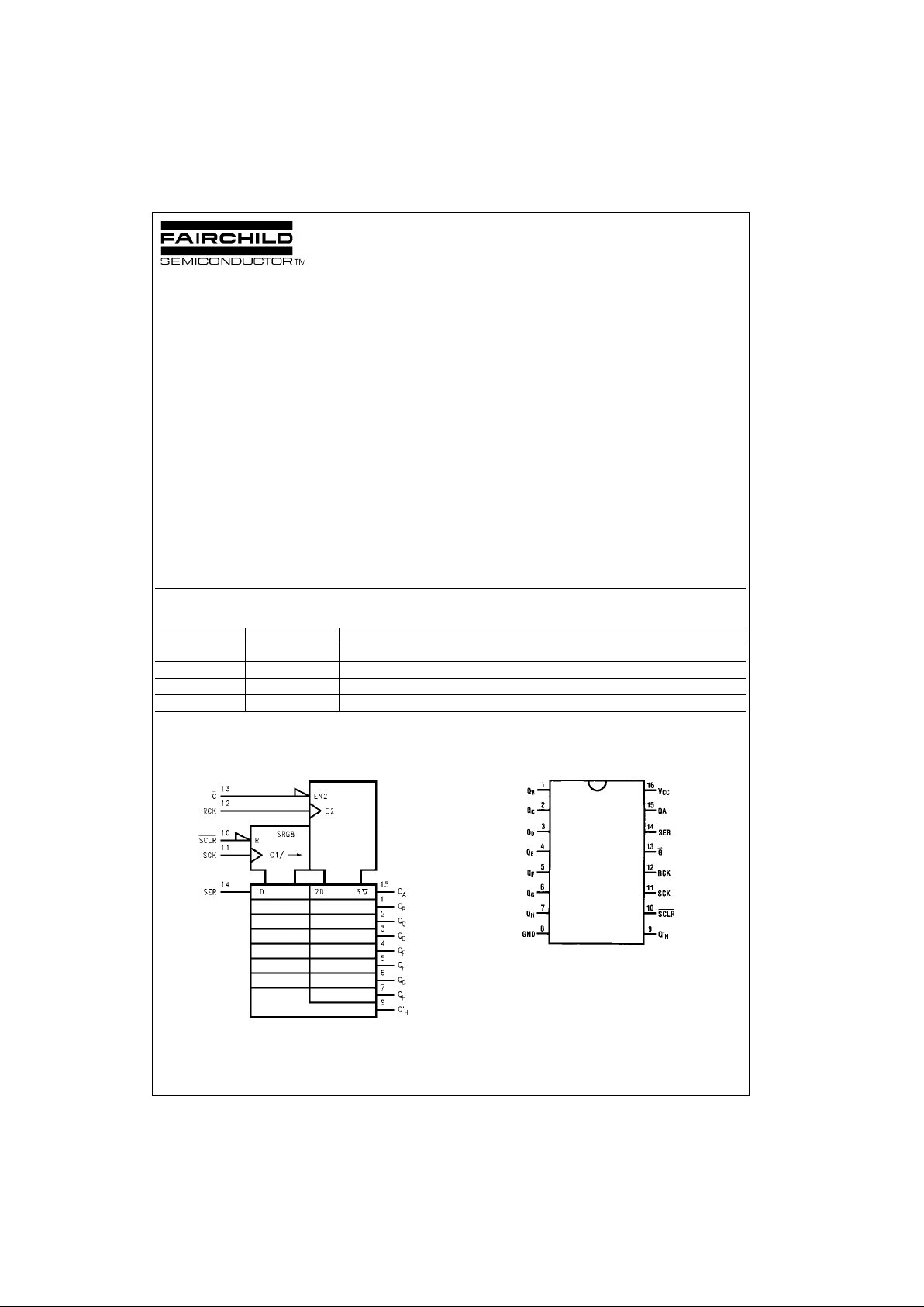
Logic Symbol
IEEE/IEC
Connection Diagram
Order Number Package Number Package Description
74VHC595M M16A 16-Lead Small Outline Integrated Circuit (SOIC), JEDEC MS-012, 0.150 Narrow
74VHC595SJ M16D 16-Lead Small Outline Package (SOP), EIAJ TYPE II, 5.3mm Wide
74VHC595MTC MTC16 16-Lead Thin Shrink Small Outline Package (TSSOP), JEDEC MO-153, 4.4mm Wide
74VHC595N N16E 16-Lead Plastic Dual-In-Line Package (PDIP), JEDEC MS-001, 0.300 Wide

www.fairchildsemi.com 2
74VHC595
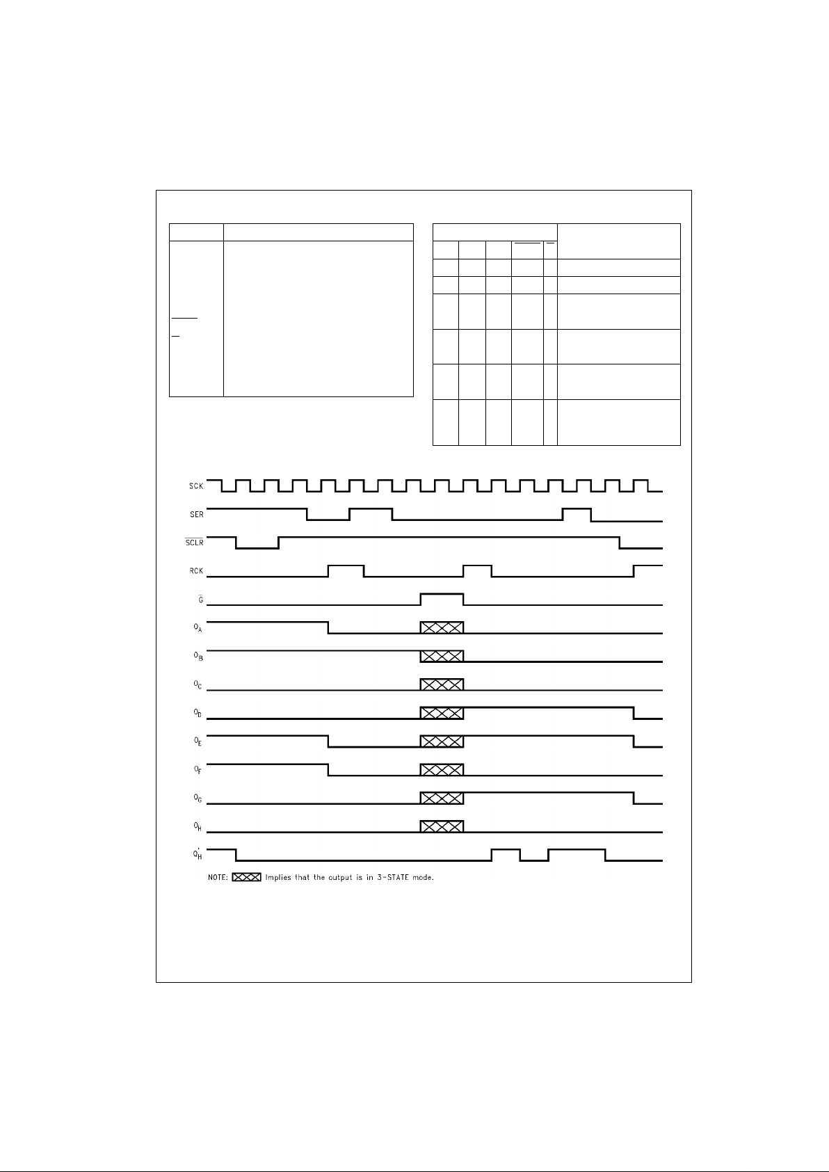
Pin Descriptions Tr uth Table
Timing Diagram
Pin Names Description
SER Serial Data Input
SCK Shift Register Clock Input
(Active rising edge)
RCK Storage Register Clock Input
(Active rising edge)
SCLR
Reset Input
G
3-STATE Output Enable Input
(Active LOW)
Q
A
- QHParallel Data Outputs
Q’
H
Serial Data Output
Inputs
Function
SER RCK SCK SCLR
G
XXX XHQA thru QH 3-STAT E
XXX XLQ
A
thru QH outputs enabled
X X X L L Shift Register cleared
Q′
H
= 0
LX↑ H L Shift Register clocked
Q
N
= Q
n-1
, Q0 = SER = L
HX↑ H L Shift Register clocked
Q
N
= Q
n-1
, Q0 = SER = H
X ↑ X H L Contents of Shift
Register transferred to
output latches

3 www.fairchildsemi.com
74VHC595
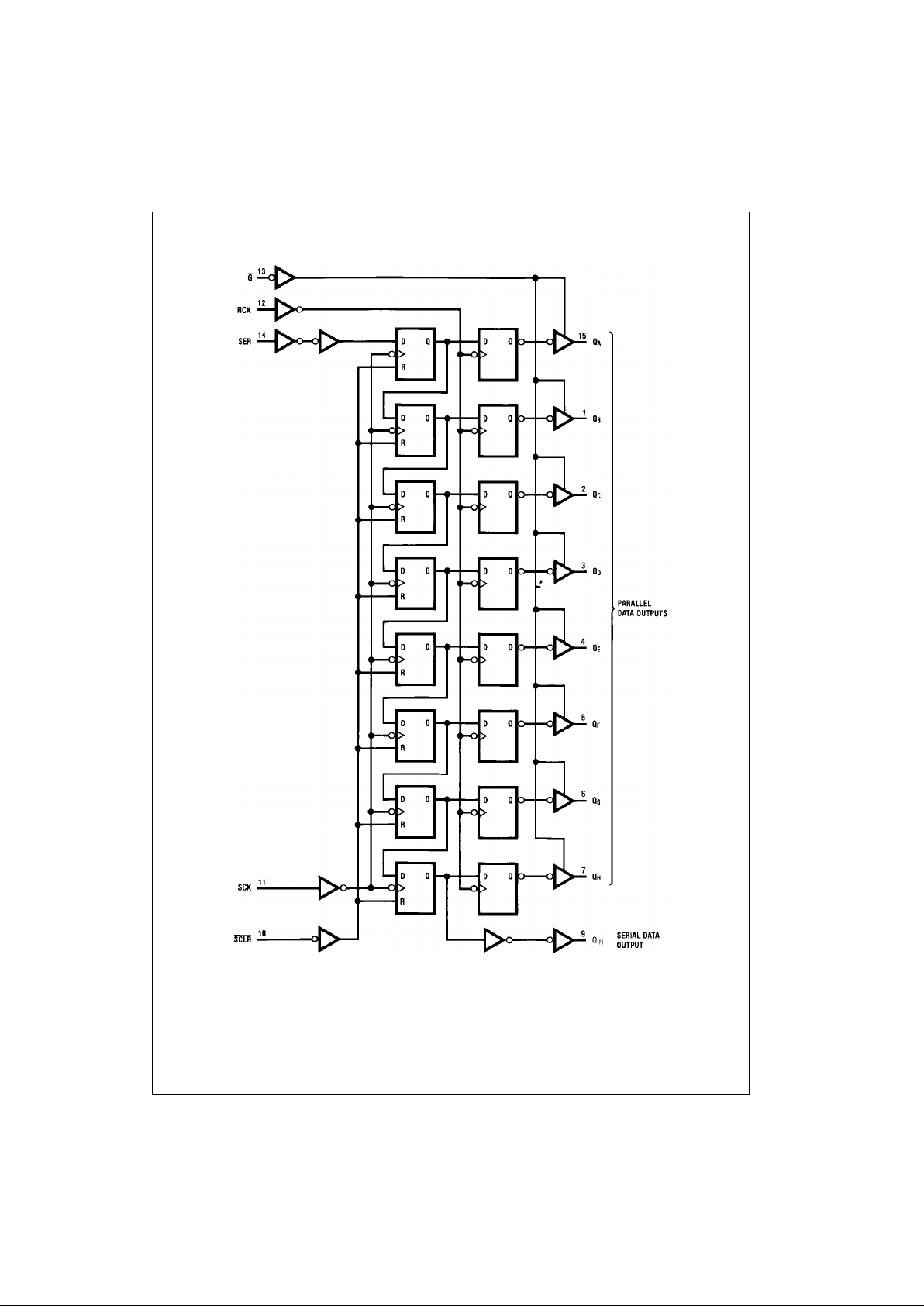
Logic Diagram
(positive logic)
 Loading...