Fairchild Semiconductor 74VHC4066WMX, 74VHC4066WM, 74VHC4066N, 74VHC4066MX, 74VHC4066MTCX Datasheet
...
© 2000 Fairchild Semiconductor Corporation DS011677 www.fairchildsemi.com
April 1994
Revised January 2000
74VHC4066 Quad Analog Switch
74VHC4066
Quad Analog Switch
General Description
These devices are digi tally controlled a nalog switches utilizing advanced silicon-gate CMOS technology. These
switches have low “on” resista nce and low “off” leakages.
They are bidirectional switches, thus any an al og inp ut m ay
be used as an output and visa-versa. Also the 4066
switches contain linearization circuitry which lowers the
“on” resistance and increases switch linearity. The 4066
devices allow control of u p to 12V (peak) analog signals
with digital control si gnals of th e same r ange. Each switch
has its own control input which disables each sw itch when
low. All analog inputs and outputs an d digital inputs are
protected from electro static damage by diodes to V
CC
and
ground.
Features
■ Typical switch enable time: 15 ns
■ Wide analog input voltage range: 0–12V
■ Low “on” resistance: 30 typ. ('4066)
■ Low quiescent current: 80 µA maximum (74VHC)
■ Matched switch characteristics
■ Individual switch controls
■ Pin and function compatible with the 74HC4066
Ordering Code:
Surface mount pack ages are also available on Tape and Reel. Specify by appending the s uffix let te r “X” to the ordering code .
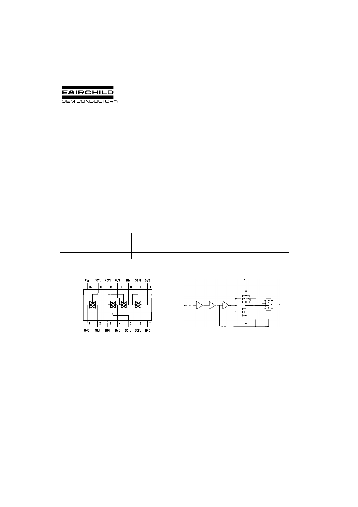
Connection Diagram
Top View
Schematic Diagram
Truth T able
Order Number Package Number Package Description
74VHC4066M M14A 14-Lead Small Outline Integrated Circuit (SOIC), JEDEC MS-120, 0.150 Narrow
74VHC4066MTC MTC14 14-Lead Thin Shrink Small Outline Package (TSSOP), JEDEC MO-153, 4.4mm Wide
74VHC4066N N14A 14-Lead Plastic Dual-In-Line Package (PDIP), JEDEC MS-001, 0.300 Wide
Input Switch
CTL I/O–O/I
L “OFF”
H“ON”

www.fairchildsemi.com 2
74VHC4066
Absolute Maximum Ratings(Note 1)
(Note 2)
Recommended Operating
Conditions
Note 1: Absolute Maximum Ratings are those values beyond which dam-
age to the device may occur.
Note 2: Unless otherwise specified all voltages are referenced to ground.
Note 3: Power Dissipation temper ature dera ting — plas tic “N” packa ge: −
12 mW/°C from 65 °C to 85°C.
DC Electrical Characteristics (Note 4)
Note 4: For a pow er supply of 5V ± 1 0% th e worst case on resistance (RON) occurs for VHC at 4.5V. Thus the 4.5V values should be used when designing
with this supply. Worst case V
IH
and VIL occur at V
CC
= 5.5V and 4.5V res pectively. (The VIH value at 5.5V is 3.85V.) The worst ca s e leakage current occ urs
for CMOS at the higher voltage and so the 5. 5V values should be used.
Note 5: At supply voltages (V
CC
– GND) ap proaching 2V the analog swit c h on resistan ce becomes ext rem ely non-linear. Ther ef ore it is recommended tha t
these devices be us ed to transmit digital only w hen using these supply v oltages.
Supply Voltage (VCC) −0.5 to +15V
DC Control Input Voltage (V
IN
) −1.5 to V
CC
+ 1.5V
DC Switch I/O Voltage (V
IO
)V
EE
− 0.5 to VCC + 0.5V
Clamp Diode Current (I
IK
, IOK) ±20 mA
DC Output Current, per pin (I
OUT
) ±25 mA
DC V
CC
or GND Current, per pin
(I
CC
) ±50 mA
Storage Temperature Range (T
STG
) −65°C to +150°C
Power Dissipation (P
D
) (Note 3) 600 mW
S.O. Package only 500 mW
Lead Temperature (T
L
)
(Soldering 10 seconds) 260°C
Min Max Units
Supply Voltage (V
CC
)212V
DC Input or Output Voltage 0 V
CC
V
(V
IN
, V
OUT
)
Operating Temperature Range (T
A
) −40 +85 °C
Input Rise or Fall Times (t
r
, tf)
V
CC
= 2.0V 1000 ns
V
CC
= 4.5V 500 ns
V
CC
= 9.0V 400 ns
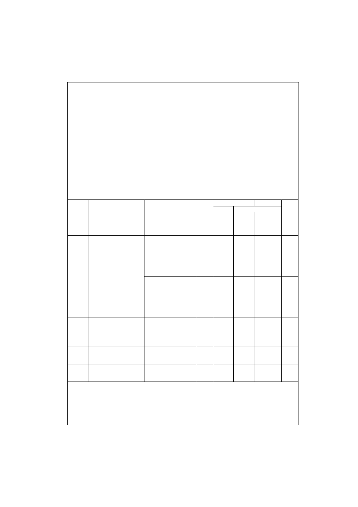
Symbol Parameter Conditions
V
CC
TA=25°CT
A
=−40 to 85°C
Units
Typ Guaranteed Limits
V
IH
Minimum HIGH Level 2.0V 1.5 1.5 V
Input Voltage 4.5V 3.15 3.15 V
9.0V 6.3 5.3 V
12.0V 8.4 8.4 V
V
IL
Maximum LOW Level 2.0V 0.5 0.5 V
Input Voltage 4.5V 1.35 1.35 V
9.0V 2.7 2.7 V
12.0V 3.6 3.6 V
R
ON
Maximum “ON” Resistance V
CTL
= VIH, IS = 2.0 mA 4.5V 100 170 200 Ω
See (Note 5) V
IS
= VCC to GND 9.0V 50 85 105 Ω
(
Figure 1
) 12.0V 30 70 85 Ω
2.0V 120 180 215 Ω
V
CTL
= VIH, IS = 2.0 mA 4.5V 50 80 100 Ω
V
IS
= VCC or GND 9.0V 35 60 75 Ω
(
Figure 1
) 12.0V 20 40 60 Ω
R
ON
Maximum “ON” Resistance V
CTL
= V
IH
4.5V 10 15 20 Ω
Matching V
IS
= VCC to GND 9.0V 5 10 15 Ω
12.0V 5 10 15 Ω
I
IN
Maximum Control V
IN
= VCC or GND ±0.05 ±0.5 µA
Input Current VCC = 2 − 6V
I
IZ
Maximum Switch “OFF” V
OS
= VCC or GND 6.0V 10 ±60 ±600 nA
Leakage Current V
IS
= GND or V
CC
9.0V 15 ±80 ±800 nA
V
CTL
= VIL (
Figure 2
) 12.0V 20 ±100 ±1000 nA
I
IZ
Maximum Switch “ON” V
IS
= VCC to GND 6.0V 10 ±40 ±150 nA
Leakage Current V
CTL
= V
IH
9.0V 15 ±50 ±200 nA
VOS = OPEN (
Figure 3
) 12.0V 20 ±60 ±300 nA
I
CC
Maximum Quiescent V
IN
= VCC or GND 6.0V 1.0 10 µA
Supply Current I
OUT
= 0 µA 9.0V 2.0 20 µA
12.0V 4.0 40 µA

3 www.fairchildsemi.com
74VHC4066
AC Electrical Characteristics
VCC = 2.0V−6.0V VEE = 0V−12V, CL = 50 pF (unless otherwise specified)
Note 6: Adjust 0 dBm for F = 1 kHz (Null RL/RON Attenuation).
Note 7: V
IS
is centered at VCC/2.
Note 8: Adjust input fo r 0 dBm.
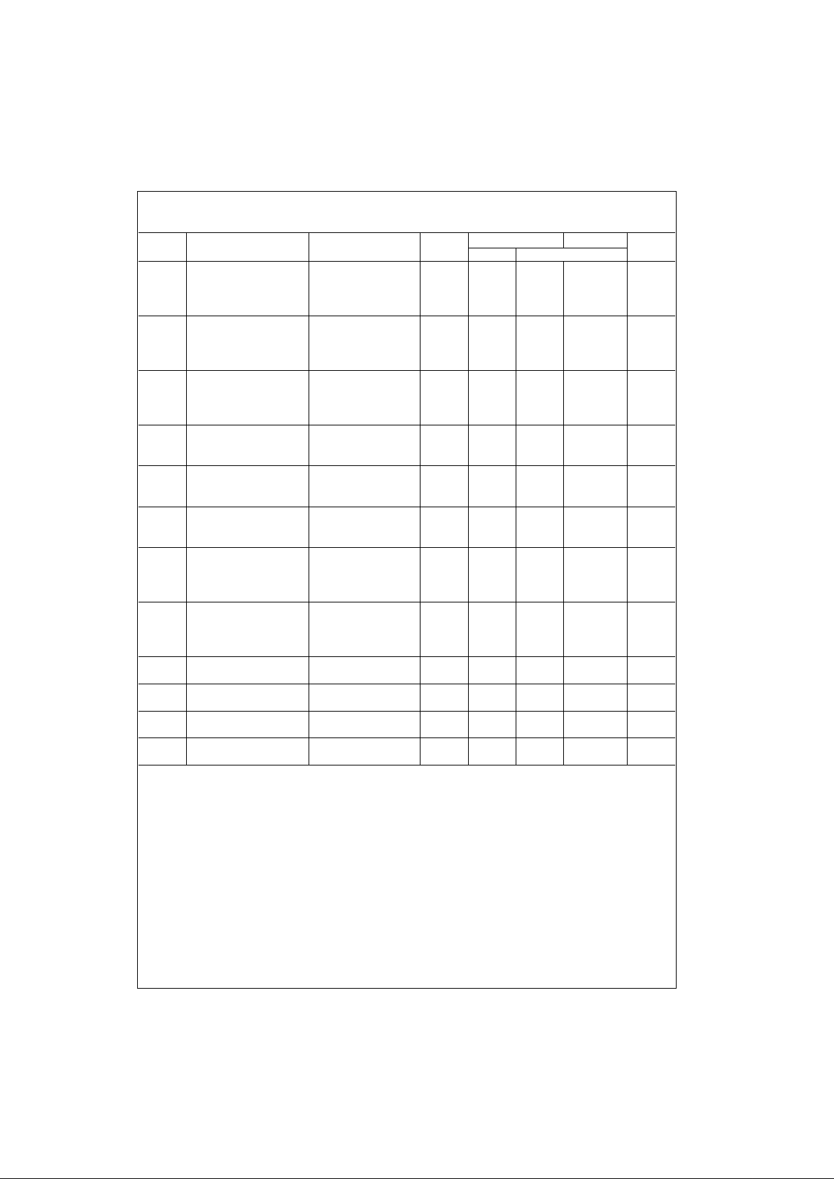
Symbol Parameter Conditions
V
CC
TA=25°CT
A
=−40 to 85°C
Units
Typ Guaranteed Limits
t
PHL
, t
PLH
Maximum Propagation 3.3V 25 30 20 ns
Delay Switch In to Out 4.5V 5 10 13 ns
9.0V 4 8 10 ns
12.0V 3 7 11 ns
t
PZL
, t
PZH
Maximum Switch Turn RL = 1 kΩ 3.3V 30 58 73 ns
“ON” Delay 4.5V 12 20 25 ns
9.0V 6 12 15 ns
12.0V 5 10 13 ns
t
PHZ
, t
PLZ
Maximum Switch Turn RL = 1 kΩ 3.3V 60 100 125 ns
“OFF” Delay 4.5V 25 36 45 ns
9.0V 20 32 40 ns
12.0V 15 30 38
Minimum Frequency RL = 600Ω 4.5V 40 MHz
Response (
Figure 7
)V
IS
= 2 VPP at (VCC/2) 9.0V 100 MHz
20 log(VO/VI) = −3 dB (Note 6)(Note 7)
Crosstalk Between RL = 600Ω, F = 1 MHz
any Two Switches (Note 7)(Note 8) 4.5V −52 dB
(
Figure 8
)9.0V−50 dB
Peak Control to Switch RL = 600Ω, F = 1 MHz 4.5V 100 mV
Feedthrough Noise CL = 50 pF 9.0V 250 mV
(
Figure 9
)
Switch OFF Signal RL = 600Ω, F = 1 MHz
Feedthrough V
(CT) VIL
Isolation (Note 7)(Note 8) 4.5V −42 dB
(
Figure 10
)9.0V−44 dB
THD Total Harmonic RL = 10 kΩ, CL = 50 pF,
Distortion F = 1 kHz
(
Figure 11
)V
IS
= 4 V
PP
4.5V .013 %
V
IS
= 8 V
PP
9.0V .008 %
C
IN
Maximum Control 5 10 10 pF
Input Capacitance
C
IN
Maximum Switch 20 pF
Input Capacitance
C
IN
Maximum Feedthrough V
CTL
= GND 0.5 pF
Capacitance
C
PD
Power Dissipation 15 pF
Capacitance
 Loading...