Fairchild Semiconductor 74VHC4046N, 74VHC4046MX, 74VHC4046MTCX, 74VHC4046MTC, 74VHC4046M Datasheet
...
April 1994
Revised April 1999
74VHC4046 CMOS Phase Lock Loop
© 1999 Fairchild Semiconductor Corporation DS011675.prf www.fairchildsemi.com
74VHC4046
CMOS Phase Lock Loop
General Description
The VHC4046 is a low power phase lock loop utilizing
advanced silicon-gate CMOS technology to obtain high frequency operation bot h in the phase com parator and VCO
sections. This device contai ns a low power linear voltage
controlled oscillator (VCO), a source follower, and three
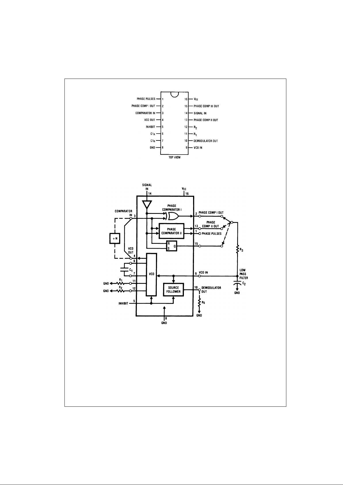
phase comparators. The thre e phase comparators ha ve a
common signal input and a common comparator input. The
signal input has a self biasing ampli fier allowing sign als to
be either capacitively co upled to the phase comparators
with a small signal or direc tly coupled with standard inp ut
logic levels. This device is similar to the CD 4046 except
that the Zener diode of the metal gate CM OS device has
been replaced with a third phase comparator.
Phase Comparator I is an exclusive OR (XOR) gate. It provides a digital error signal that maintai ns a 90 phase shift
between the VCO’s center freque ncy and the input signal
(50% duty cycle input waveforms). This ph ase detector is
more susceptible to locking onto harmonics of the input frequency than phase comparator I, but pr ovi de s bet ter n oi se
rejection.
Phase comparator III is an S R fli p -flop ga te. It can b e used
to provide the phase co mp ara tor fun cti on s an d is similar to
the first comparator in performance.
Phase comparator II is an edge se nsitive digit al seque ntial
network. Two signal outputs are provided, a comparator
output and a phase pulse output. The comparator output is
a 3-STA TE output that provides a signal that locks the VCO
output signal to the i n pu t sign al with 0 phase shift b etwe en
them. This comparator is more susceptible to noise throw-
ing the loop out of lock, but is less likely to lock onto h armonics than the other two comparators.
In a typical application a ny one of the three comparator s
feed an external filter network which in tur n f eed s th e VCO
input. This input is a very high impedance CMOS input
which also drives the source follower. The VCO’s operating
frequency is set by three external components co nnected
to the C1
A
, C1B, R1 and R2 pins. An inhibit pi n is p rovi ded
to disable the VCO and the source follower, providing a
method of putting the IC in a low power state.
The source follower is a MOS transistor whose gate is connected to the VCO input and whose drain connects the
Demodulator output. This output normally i s used by tying
a resistor from pin 10 to ground , and provi des a means o f
looking at the VCO input without loading down modifying
the characteristics of the PLL filter.
Features
■ Low dynamic power consumption: (V
CC
= 4.5V)
■ Maximum VCO operating frequency: 12 MHz
(V
CC
= 4.5V)
■ Fast comparator response time (V
CC
= 4.5V)
Comparator I: 25 ns
Comparator II: 30 ns
Comparator III: 25 ns
■ VCO has high linearity and high temperature stability
■ Pin and function compatible with the 74HC4046
Ordering Code:
Surface mount pack ages are also available on Tape and Reel. Specify by appending the s uffix let te r “X” to the ordering code .
Order Number Package Number Package Description
74VHC4046M M16A 16-Lead Small Outline Integrated Circuit (SOIC), JEDEC MS-012, 0.150 Narrow
74VHC4046MTC MTC16 16-Lead Thin Shrink Small Outline Package (TSSOP), JEDEC MO-153, 4.4mm Wide
74VHC4046N N16E 16-Lead Plastic Dual-In-Line Package (PDIP), JEDEC MS-001, 0.300 Wide

www.fairchildsemi.com 2
74VHC4046
Connection Diagram
Block Diagram

3 www.fairchildsemi.com
74VHC4046
Absolute Maximum Ratings(Note 1)
(Note 2)
Recommended Operating
Conditions
Note 1: Maximum Ratings are those values beyond which damage to the
device may occur.
Note 2: Unless otherwise specified all voltages are referenced to ground.
Note 3: Power Dissipation temperature derat ing — plastic “N” package: −
12 mW/°C from 65°C to 85°C.
DC Electrical Characteristics (Note 4)
Note 4: For a pow er supply of 5V ±10% the worst case output voltages (VOH, and VOL) occur for VHC at 4.5V. Thus the 4.5V values should be used when
designing with this supply. Worst case V
IH
and VIL occur at V
CC
= 5.5V and 4.5V respectively. (The VIH value at 5.5V is 3 .8 5V.) The worst c as e leakage cur-
rent (I
IN
, ICC, and IOZ) occur for CMOS at the higher voltage and so th e 6. 0V values should be used.
Supply Voltage (VCC) −0.5 to + 7.0V
DC Input Voltage (V
IN
) −1.5 to VCC +1.5V
DC Output Voltage (V
OUT
) −0.5 to VCC + 0.5V
Clamp Diode Current (I
IK
, IOK) ±20 mA
DC Output Current per pin (I
OUT
) ±25 mA
DC V
CC
or GND Current,
per pin (I
CC
) ±50 mA
Storage Temperature Range (T
STG
) −65°C +150°C
Power Dissipation (P
D
)
(Note 3) 600 mW
S.O. Package only 500 mW
Lead Temperature (T
L
)
(Soldering 10 seconds) 260°C
Min Max Units
Supply Voltage (V
CC
)26V
DC Input or Output Voltage 0 V
CC
V
(V
IN
, V
OUT
)
Operating Temperature Range (T
A
) −40 +85 °C
Input Rise or Fall Times
(t
r
, tf)V
CC
= 2.0V 1000 ns
V
CC
= 4.5V 500 ns
V
CC
= 6.0V 400 ns
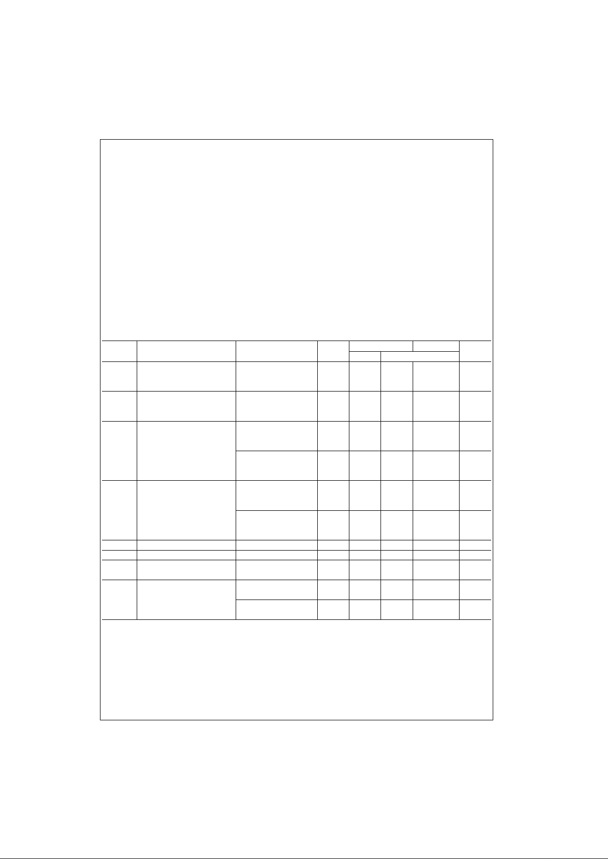
Symbol Parameter Conditions
V
CC
TA=25°CTA=−40 to 85°C
Units
Typ Gu a ra nt eed Lim its
V
IH
Minimum HIGH Level 2.0V 1.5 1.5 V
Input Voltage 4.5V 3.15 3.15 V
6.0V 4.2 4.2 V
V
IL
Maximum LOW Level 2.0V 0.5 0.5 V
Input Voltage 4.5V 1.35 1.35 V
6.0V 1.8 1.8 V
V
OH
Minimum HIGH Level V
IN
= VIH or V
IL
2.0V 2.0 1.9 1.9 V
Output Voltage |I
OUT
| ≤ 20 µA 4.5V 4.5 4.4 4.4 V
6.0V 6.0 5.9 5.9 V
V
IN
= VIH or V
IL
|I
OUT
| ≤ 4.0 mA 4.5V 4.2 3.98 3.84 V
|I
OUT
| ≤ 5.2 mA 6.0V 5.7 5.48 5.34 V
V
OL
Maximum LOW Level V
IN
= VIH or V
IL
2.0V 0 0.1 0.1 V
Output Voltage |I
OUT
| ≤ 20 µA4.5V00.10.1V
6.0V 0 0.1 0.1 V
V
IN
= VIH or V
IL
|I
OUT
| ≤ 4.0 mA 4.5V 0.2 0.26 0.33 V
|I
OUT
| ≤ 5.2 mA 6.0V 0.2 0.26 0.33 V
I
IN
Maximum Input Current (Pins 3,5,9) V
IN
= VCC or GND 6.0V ±0.1 ±1.0 µA
I
IN
Maximum Input Current (Pin 14) V
IN
= VCC or GND 6.0V 20 50 80 µA
I
OZ
Maximum 3-STATE Output V
OUT
= VCC or GND 6.0V ±0.25 ±2.5 µA
Leakage Current (Pin 13)
I
CC
Maximum Quiescent Supply V
IN
= VCC or GND 6.0V 30 40 65 µA
Current I
OUT
= 0 µA
VIN = VCC or GND 6.0V 600 750 1200 µA
Pin 14 Open

www.fairchildsemi.com 4
74VHC4046
AC Electrical Characteristics
V
CC
= 2.0 to 6.0V, CL = 50 pF, tr = t
f
= 6 ns (unless otherwise specified.)
Symbol Parameters Conditions
V
CC
TA=25C TA=−40 to 85°C
Units
Typ Guaranteed Limits
AC Coupled C (series) = 100 pF 2.0V 25 100 150 mV
Input Sensitivity, f
IN
= 500 kHz 4.5V 50 150 200 mV
Signal In 6.0V 135 250 300 mV
tr, t
f
Maximum Output 2.0V 30 75 95 ns
Rise and Fall Time 4.5V 9 15 19 ns
6.0V 8 12 15 ns
C
IN
Maximum Input 7 pF
Capacitance
Phase Comparator I
t
PHL
, t
PLH
Maximum Propagation 3.3V 65 117 146 ns
Delay 4.5V 25 40 50 ns
6.0V 20 34 43 ns
Phase Comparator II
t
PZL
Maximum 3-STATE 3.3V 75 130 160 ns
Enable Time 4.5V 25 45 56 ns
6.0V 22 38 48 ns
t
PZH
, t
PHZ
Maximum 3-STATE 3.3V 88 140 175 ns
Enable Time 4.5V 30 48 60 ns
6.0V 25 41 51 ns
t
PLZ
Maximum 3-STATE 3.3V 90 140 175 ns
Disable Time 4.5V 32 48 60 ns
6.0V 28 41 51 ns
t
PHL
, t
PLH
Maximum Propagation 3.3V 100 146 180 ns
Delay HIGH-to-LOW 4.5V 34 50 63 ns
to Phase Pulses 6.0V 27 43 53 ns
Phase Comparator III
t
PHL
, t
PLH
Maximum Propagation 3.3V 75 117 146 ns
Delay 4.5V 25 40 50 ns
6.0V 22 34 43 ns
C
PD
Maximum Power All Comparators 130 pF
Dissipation VIN = VCC and GND
Capacitance
Voltage Controlled Oscillator (Specified to operate from V
CC
= 3.0V to 6.0V)
f
MAX
Maximum C1 = 50 pF
Operating R1 = 100Ω 4.5V 7 4.5 MHz
Frequency R2 = ∞ 6.0V 11 7 MHz
VCOin = V
CC
C1 = 0 pF 4.5V 12 MHz
R1 = 100Ω 6.0 14 MHz
VCOin = V
CC
Duty Cycle 50 %
Demodulator Output
Offset Voltage Rs = 20 kΩ 4.5V 0.75 1.3 1.5 V
VCOin–V
dem
Offset Rs = 20 kΩ 4.5V
Variation VCOin = 1.75V 0.65 V
2.25V 0.1
2.75V 0.75

5 www.fairchildsemi.com
74VHC4046
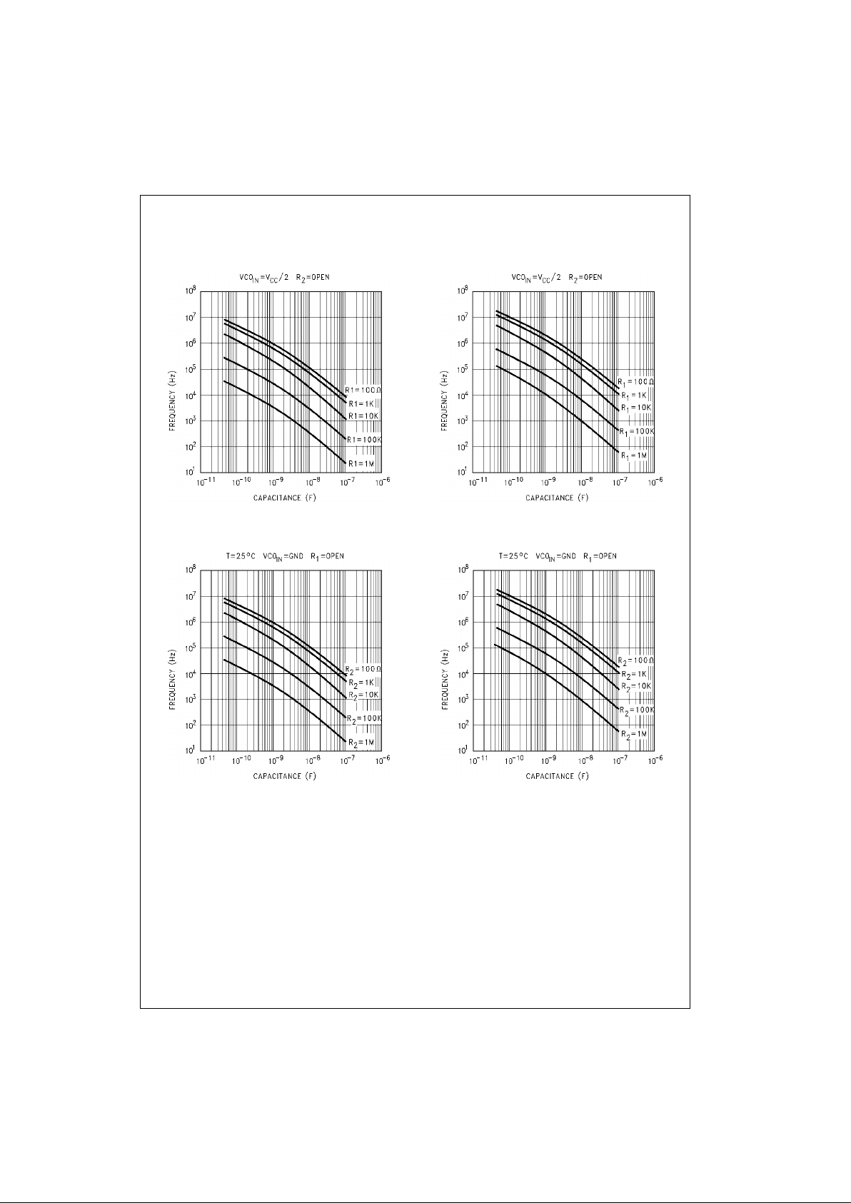
Typical Performance Characteristics
Typical Center Frequency
vs R
1
, C1VCC = 4.5V
Typical Center Frequency
vs R1, C1VCC = 6V
Typical Offset Frequency
vs R
2
, C1VCC = 4.5V
Typical Offset Frequency
vs R2, C1VCC = 6V
 Loading...