Fairchild Semiconductor 74VHC245SJX, 74VHC245SJ, 74VHC245N, 74VHC245MX, 74VHC245MTCX Datasheet
...
November 1992
Revised March 1999
74VHC245 Octal Bidirectional Transceiver with 3-STAT E Outputs
© 1999 Fairchild Semiconductor Corporation DS011520.prf www.fairchildsemi.com
74VHC245
Octal Bidirectional Transceiver with 3-STATE Outputs
General Description
The VHC245 is an advanced high sp eed CMOS octal b us
transceiver fabricated with silicon gate CMOS technology.
It achieves high speed operation similar to equivalent Bipolar Schottky TTL while maintaining the CMOS low power
dissipation. The VHC245 i s int end ed for bidirectional asynchronous communication be tween dat a buss es. The dire ction of data transmissio n is determined by the le vel of the
T/R
input. The enable inp ut can be used to disable the
device so that the busses are effectively isolated. All inputs
are equipped with protection circuits against static discharge.
Features
■ High Speed: tPD = 4.0 ns (typ) at VCC = 5V
■ High Noise Immunity: V
NIH
= V
NIL
= 28% VCC (Min)
■ Power Down Protection is provided on all inputs
■ Low Noise: V
OLP
= 0.9V (typ)
■ Low Power Dissipation:
I
CC
= 4 µA (Max) @ TA = 25°C
■ Pin and Function Compatible with 74HC245
Ordering Code:
Surface mount pack ages are also available on Tape and Reel. Specify by appending the s uffix let te r “X” to the ordering code .
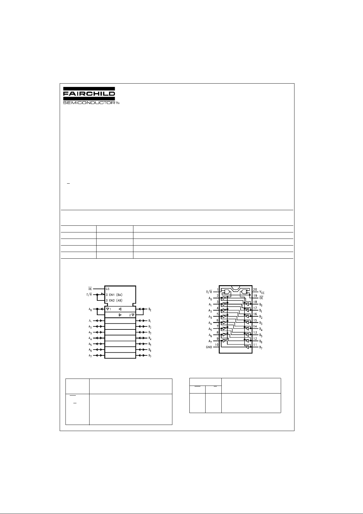
Logic Symbol
IEEE/IEC
Pin Description
Connection Diagram
Truth Table
H = HIGH Voltage Level L = LOW Voltage Level X = Immaterial
Any unused bus terminals during HIGH-Z St ate must be held HIGH or
LOW.
Order Number Package Number Package Description
74VHC245M M20B 20-Lead Small Outline Integrated Package (SOIC), JEDEC MS-013, 0.300” Wide
74VHC245SJ M20D 20-Lead Small Outline Package (SOP), EIAJ TYPE II, 5.3mm Wide
74VHC245MTC MTC20 20-Lead Thin Shrink Small Outline Package (TSSOP), JEDEC MO-153, 4.4mm Wide
74VHC245N N20A 20-Lead Plastic Dual-In-Line Package (PDIP), JEDEC MS-001, 0.300” Wide
Pin Description
Names
OE
Output Enable Input
T/R
Transmit/Receive Input
A
0–A7
Side A Inputs or 3-STATE Outputs
B
0–B7
Side B Inputs or 3-STATE Outputs
Inputs Outputs
OE
T/R
L L Bus B Data to Bus A
L H Bus A Data to Bus B
HXHIGH-Z State

www.fairchildsemi.com 2
74VHC245
Absolute Maximum Ratings(Note 1) Recommended Operating
Conditions
(Note 2)
Note 1: Absolute Maximum Ratings are values beyond which the device
may be damaged or ha ve its useful li fe impaire d. The datab ook specifications should be met, without exception, to ensure that the system design is
reliable over its p ower supp ly, temperature, and ou tput/input loading variables. Fairchild does not recom mend operation outside databook specifications.
Note 2: Unused inputs or I/O pins must be held HIGH or LOW. They may
not float.
DC Electrical Characteristics
Supply Voltage (VCC) −0.5V to +7.0V
DC Input Voltage (V
IN
) (T/R, OE) −0.5V to 7.0V
DC Output Voltage (V
OUT
) −0.5V to VCC + 0.5V
Input Diode Current (I
IK
) (T/R, OE) −20 mA
Output Diode Current (I
OK
) ±20 mA
DC Output Current (I
OUT
) ±25 mA
DC V
CC
/GND Current (ICC) ±75 mA
Storage Temperature (T
STG
) −65°C to +150°C
Lead Temperature (T
L
)
(Soldering, 10 seconds) 260°C
Supply Voltage (V
CC
) 2.0V to 5.5V
Input Voltage (V
IN
)(T/R, OE)0V to 5.5V
Output Voltage (V
OUT
) 0V to V
CC
Operating Temperature (T
OPR
) −40°C to +85°C
Input Rise and Fall Time (t
r
, tf)
V
CC
= 3.3V ± 0.3V 0 ∼ 100 ns/V
V
CC
= 5.0V ± 0.5V 0 ∼ 20 ns/V
Symbol Parameter
V
CC
(V)
TA = 25°CT
A
= −40°C to +85°C
Units Conditions
Min Typ Max Min Max
V
IH
HIGH Level 2.0 1.50 1.50
V
Input Voltage 3.0 − 5.5 0.7 V
CC
0.7 V
CC
V
IL
LOW Level 2.0 0.50 0.50
V
Input Voltage 3.0 − 5.5 0.3 V
CC
0.3 V
CC
V
OH
HIGH Level 2.0 1.9 2.0 1.9 VIN = VIHIOH = −50 µA
Output Voltage 3.0 2.9 3.0 2.9 V or V
IL
4.5 4.4 4.5 4.4
3.0 2.58 2.48
V
IOH = −4 mA
4.5 3.94 3.80 IOH = −8 mA
V
OL
LOW Level 2.0 0.0 0.1 0.1 VIN = VIHIOL = 50 µA
Output Voltage 3.0 0.0 0.1 0.1 V or V
IL
4.5 0.0 0.1 0.1
3.0 0.36 0.44
V
IOL = 4 mA
4.5 0.36 0.44 IOL = 8 mA
I
OZ
3-STATE Output VIN = VCC or GND
Off-State Current 5.5 ±0.25 ±2.5 µAV
OUT
= VCC or GND
VIN OE = VIH or V
IL
I
IN
Input Leakage 0 − 5.5 ±0.1 ±1.0 µAVIN = 5.5V or GND
(T/R, OE)
Current
I
CC
Quiescent Supply Current 5.5 4.0 40.0 µAVIN = VCC or GND
 Loading...