Fairchild Semiconductor 74VHC153SJ, 74VHC153N, 74VHC153MX, 74VHC153MTCX, 74VHC153MTC Datasheet
...
August 1993
Revised April 1999
74VHC153 Dual 4-Input Multiplexer
© 1999 Fairchild Semiconductor Corporation DS011634.prf www.fairchildsemi.com
74VHC153
Dual 4-Input Multiplexer
General Description
The VHC153 is an advanced high-speed CMOS device
fabricated with silicon gate CMOS technology. It achieves
the high-speed operation similar to equivalent Bipolar
Schottky TTL while maintaining the CMOS low power dissipation. The VHC153 i s a high-speed Dual 4-Input Multiplexer with common select inputs and individual enable
inputs for each section. It can select two lines of d ata fro m
four sources. The t wo buffered outpu ts pre sen t data in t he
true (non-inverted) form. In addition to multipl exer operation, the VHC153 can act as a function generator a nd generate any two functions of three variables. An input
protection circuit insure s that 0V to 7V can be applied to
the input pins without regard to the suppl y voltage. This
device can be used to in terface 5V to 3V sys tems an d two
supply systems such as battery backup. This circuit prevents device destruction due to mismatched supply and
input voltages.
Features
■ High Speed: tPD = 5.0 ns at TA = 25°C
■ Low power dissipation: I
CC
= 4 µA (max) at TA = 25°C
■ High noise immunity: V
NIH
= V
NIL
= 28% VCC (min)
■ Power down protection is provided on all inputs
■ Pin and function compatible with 74HC153
Ordering Code:
Surface mount pack ages are also available on Tape and Reel. Specify by appending the s uffix let te r “X” to the ordering code .
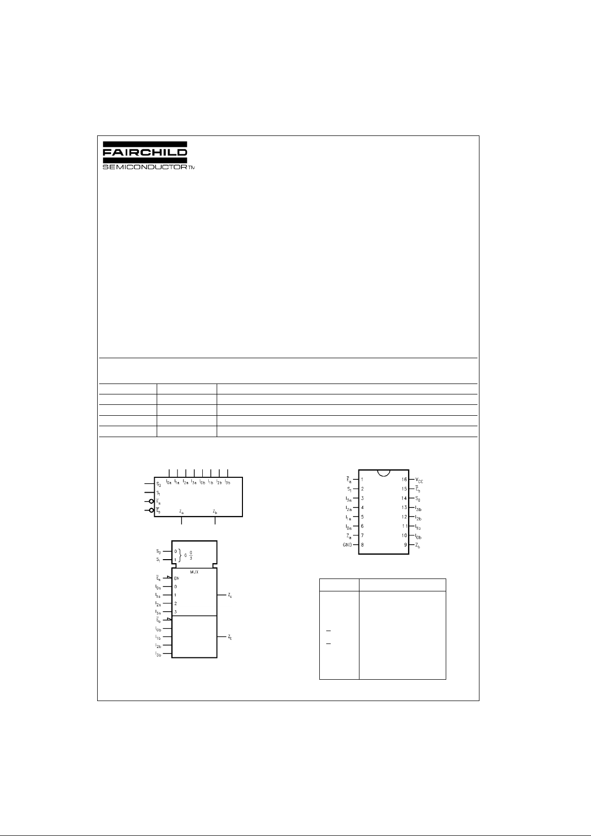
Logic Symbols
IEEC/IEC
Connection Diagram
Pin Descriptions
Order Number Package Number Package Description
74VHC153M M16A 16-Lead Small Outline Integrated Circuit (SOIC), JEDEC MS-012, 0.150 Narrow
74VHC153SJ M16D 16-Lead Small Outline Package (SOP), EIAJ TYPE II, 5.3mm Wide
74VHC153MTC MTC16 16-Lead Thin Shrink Small Outline Package (TSSOP), JEDEC MO-153, 4.4mm Wide
74VHC153N N16E 16-Lead Plastic Dual-In-Line Package (PDIP), JEDEC MS-001, 0.300 Wide
Pin Names Description
I
0a–I3a
Side A Data Inputs
I
0b–I3b
Side B Data Inputs
S
0
, S
1
Common Select Inputs
E
a
Side A Enable Input
E
b
Side B Enable Input
Z
a
Side A Output
Z
b
Side B Output

www.fairchildsemi.com 2
74VHC153
Functional Description
The VHC153 is a dual 4-input multiplexer. It can select two
bits of data from up to four sources under the control of the
common Select inputs (S
0
, S1). The two 4-input multiplexer
circuits have individ ua l acti ve -LO W En ab les (E
a
, Eb) which
can be used to strobe the outputs independently. When the
Enables (E
a
, Eb) are HIGH, the cor resp on ding ou tpu t s ( Za,
Z
b
) are forced LOW. The VHC153 is the lo gic implementa-
tion of a 2-pole, 4-position switch, where the position of the
switch is determined by the logic levels supplied to the
Select inputs. The logic equations for the outputs are
shown below.
Z
a
= Ea • (I0a • S1 • S0 + I1a • S1 • S0 +
I
2a
• S1 • S0 + I3a • S1 • S0)
Z
b
= Eb • (I0b • S1 • S0 + I1b • S1 • S0 +
I
2b
• S1 • S0 + I3b • S1 • S0)
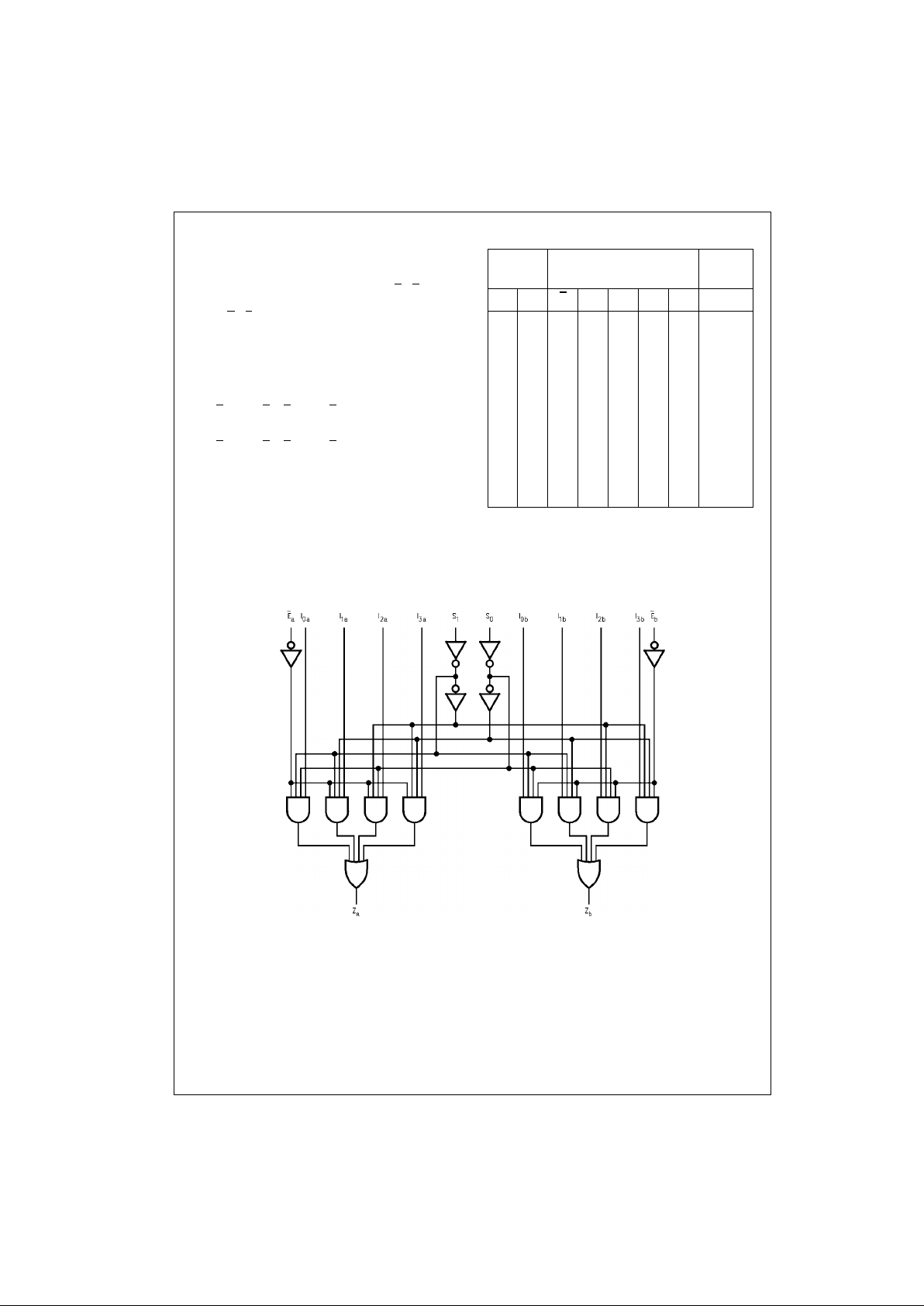
Tr uth Table
H = HIGH Voltage Level
L = LOW Voltage Level
X = Immaterial
Logic Diagram
Please note that this diagram is provided o nly f or t he understanding of logic operations and shou ld not be used to estimate pro pagation delays.
Select
Inputs (a or b) Output
Inputs
S
0S1
E I0I1I2I
3
Z
XXHXXXX L
LLLLXXX L
LLLHXXX H
HLLXLXX L
HLLXHXX H
LHLXXLX L
LHLXXHX H
HHLXXXL L
HHLXXXH H

3 www.fairchildsemi.com
74VHC153
Absolute Maximum Ratings(Note 1) Recommended Operating
Conditions
(Note 2)
Note 1: Absolute maximum ratings are those values beyon d which the
device may be damaged or have its us eful life impaired. The d atabook
specifications should be met, without exception, to ensure that the system
design is reliable over its power supply, temperature, and output/input loading variables. F airchild does not recommend oper ation outside datab ook
specifications.
Note 2: Unused inputs must be held HIGH or LOW. They may not float.
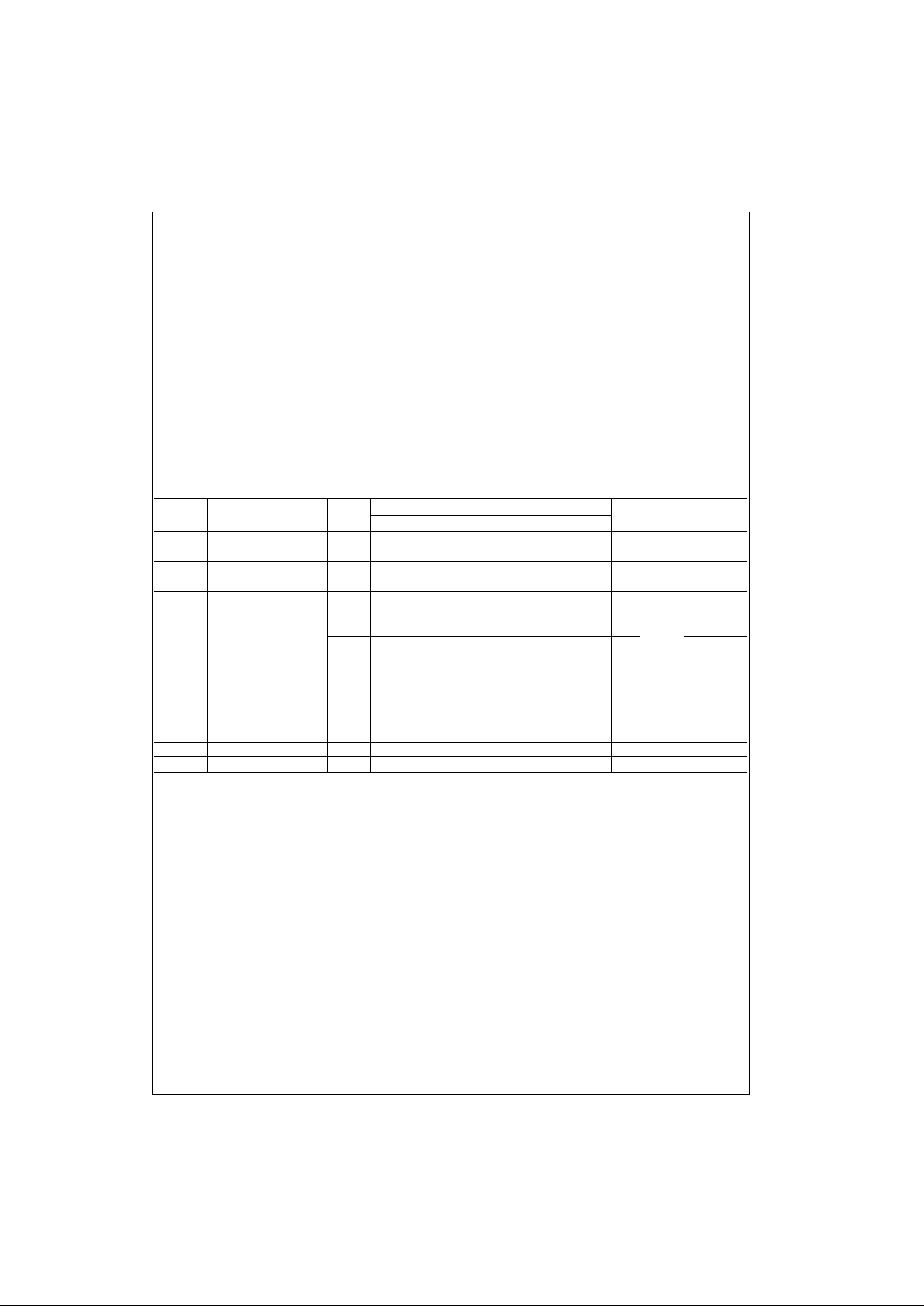
DC Electrical Characteristics
Supply Voltage (VCC) −0.5V to +7.0V
DC Input Voltage (V
IN
) −0.5V to + 7.0V
DC Output Voltage (V
OUT
) −0.5V to VCC + 0.5V
Input Diode Current (I
IK
) −20 mA
Output Diode Current (I
OK
) ±20 mA
DC Output Current (I
OUT
) ±25 mA
DC V
CC
/GND Current (ICC) ±50 mA
Storage Temperature (T
STG
) −65°C to +150°C
Lead Temperature (T
L
)
(Soldering, 10 seconds) 260°C
Supply Voltage (V
CC
) 2.0V to 5.5V
Input Voltage (V
IN
)0V to +5.5
Output Voltage (V
OUT
)0V to V
CC
Operating Temperature (T
OPR
) −40°C to +85°C
Input Rise and Fall Time (t
r
, tf)
V
CC
= 3.3V ± 0.3V 0∼100 ns/V
V
CC
= 5.0V ± 0.5V 0∼20 ns/V
Symbol Parameter
V
CC
(V)
TA = 25°CT
A
= −40°C to +85°C
Units Conditions
Min Typ Max Min Max
V
IH
HIGH Level Input 2.0 1.50 1.50
V
Voltage 3.0 − 5.5 0.7 V
CC
0.7 V
CC
V
IL
LOW Level Input 2.0 0.50 0.50
V
Voltage 3.0 − 5.5 0.3 V
CC
0.3 V
CC
V
OH
HIGH Level Output 2.0 1.9 2.0 1.9 VIN = VIHIOH = −50 µA
Voltage 3.0 2.9 3.0 2.9 V or V
IL
4.5 4.4 4.5 4.4
3.0 2.58 2.48
V
IOH = −4 mA
4.5 3.94 3.80 IOH = −8 mA
V
OL
LOW Level Output 2.0 0.0 0.1 0.1 VIN = VIHIOL = 50 µA
Voltage 3.0 0.0 0.1 0.1 V or V
IL
4.5 0.0 0.1 0.1
3.0 0.36 0.44
V
IOL = 4 mA
4.5 0.36 0.44 IOL = 8 mA
I
IN
Input Leakage Current 0 − 5.5 ±0.1 ±1.0 µAVIN = 5.5V or GND
I
CC
Quiescent Supply Current 5.5 4.0 40.0 µAVIN = VCC or GND
 Loading...