Fairchild Semiconductor 74VHC139SJX, 74VHC139SJ, 74VHC139CW, 74VHC139N, 74VHC139MX Datasheet
...
November 1992
Revised April 1999
74VHC139 Dual 2-to-4 Decoder/Demultiplexer
© 1999 Fairchild Semiconductor Corporation DS011521.prf www.fairchildsemi.com
74VHC139
Dual 2-to-4 Decoder/Demultiplexer
General Description
The VHC139 is an adva nced hig h sp eed C MO S D ua l 2-t o4 Decoder/Demultiplexer fabricated with silicon gate
CMOS technology. It achieves the high speed operation
similar to equivalent Bipolar Schottky TTL while maintaining the CMOS low power dissipation.
The active LOW enable input ca n be used for gating or it
can be used as a data input for demultiplexing applications.
When the enable input is held HIGH, all four outputs are
fixed at a HIGH logic level inde pen de nt of the other inputs.
An input protection circuit en sures that 0V to 7V can be
applied to the input pins without re gard to the supply volt-
age. This device can be used to interface 5V to 3V systems
and two supply systems such as ba ttery back up . This circuit prevents device destruction due to m isma tche d supply
and input voltages.
Features
■ High Speed: tPD = 5.0 ns (typ) at TA = 25°C
■ Low power dissipation: I
CC
= 4 µA (Max.) at TA = 25°C
■ High noise immunity: V
NIH
= V
NIL
= 28% VCC (Min.)
■ Power down protection is provided on all inputs
■ Pin and function compatible with 74HC139
Ordering Code:
Surface mount pack ages are also available on Tape and Reel. Specify by appending the s uffix let te r “X” to the ordering code.
Connection Diagram Pin Description
Truth Table
H = HIGH Voltage Level
L = LOW Voltage Level
X = Immaterial
Order Number Package Number Package Description
74VHC139M M16A 16-Lead Small Outline Integrated Circuit (SOIC), JEDEC MS-012, 0.150” Narrow
74VHC139SJ M16D 16-Lead Small Outline Package (SOP), EIAJ TYPE II, 5.3mm Wide
74VHC139MTC MTC16 16-Lead Thin Shrink Small Outline Package (TSSOP), JEDEC MO-153, 4.4mm Wide
74VHC139N N16E 16-Lead Plastic Dual-In-Line Package (PDIP), JEDEC MS-001, 0.300” Wide
Pin Names Description
A
0
, A
1
Address Inputs
E
Enable Inputs
O
0–O3
Outputs
Inputs Outputs
E
A
0
A
1
O
0
O
1
O
2
O
3
HXXHHHH
LLLLHHH
LHLHLHH
LLHHHLH
LHHHHHL

www.fairchildsemi.com 2
74VHC139
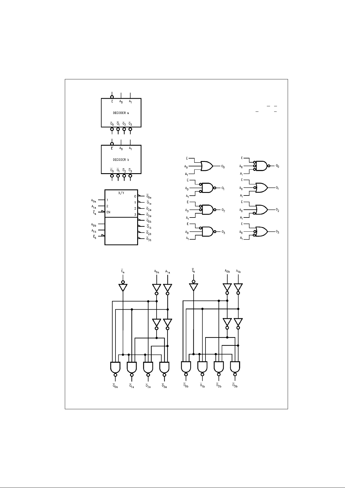
Logic Symbols
IEEE/IEC
Functional Description
The VHC139 is a high-spe ed dual 2-to-4 de coder/demul tiplexer. The device has two independent decode rs, each of
which accepts two binary weighted inputs (A
0–A1
) and pro-
vides four mutually exclusive active-LOW outputs (O
0–O3
).
Each decoder has an active-LOW enable (E
). When E is
HIGH all outputs are forced HIGH. The enable can be used
as the data input for a 4-output demu ltiplexer applicat ion.
Each half of the VHC1 39 generates all four minterms of
two variables. These four minterms are useful in some
applications, replacin g multip le gate fun ctions as sho wn in
Figure 1
, and thereby reduc ing the number of packages
required in a logic network.
FIGURE 1. Gate Functions (Each Half)
Logic Diagram
Please note that this diagram is provided only f or t he understanding of logic operations and should not be used to estimate propagation delays.
 Loading...