

Fairchild Semiconductor 74VCXH162374MTX, 74VCXH162374MTD Datasheet
January 2000
Revised March 2000
74VCXH162374
Low Voltage 16-Bit D-Type Flip-Flop with Bushold
and 26Ω Series Resistors in Outputs
74VCXH162374 Low Voltage 16-Bit D-Type Flip-Flop with Bushold
General Description
The VCXH162374 contains sixteen non-inverting D-type
flip-flops with 3-STATE outputs and is intended for bus oriented applications. The dev ice is byte controlled. A buffered clock (CP) and ou tput enable (OE
each byte and can be shorted together for full 16-bit operation.
The VCXH162374 data inputs include activ e bushold circuitry, eliminating the need for external pull-up resistors to
hold unused or floating data inputs at a valid logic level.
The 74VCXH162374 is also designed with 26Ω series
resistors in the outputs. This design reduce s line noise in
applications such as memory address drivers, clock drivers
and bus transceivers/transmitters.
The 74VCXH16237 4 is desig ned for lo w voltage (1.65V to
3.6V) V
The 74VCXH162374 is fabricated with an advanced CMOS
technology to achieve high speed operation while maintaining low CMOS power dissipation.
applications with output compatibility up to 3.6V.
CC
) are common to
Features
■ 1.65V–3.6V VCC supply operation
■ 3.6V tolerant control inputs and outputs
■ Bushold data inputs eliminates the need for external
pull-up/pull-down resistors
■ 26Ω series resistors in outputs
(CLK to On)
■ t
PD
3.4 ns max for 3.0V to 3.6V V
4.8 ns max for 2.3V to 2.7V V
9.6 ns max for 1.65V to 1.95V V
■ Static Drive (IOH/IOL)
±12 mA @ 3.0V V
±8 mA @ 2.3V V
±3 mA @ 1.65V V
■ Uses patented noise/EMI reduction circuitry
■ Latch-up performance exce eds 300 mA
■ ESD performance:
Human body model > 2000V
Machine model > 200V
CC
CC
CC
CC
CC
CC
Ordering Code:
Order Number
74VCXH162374MTD MTD48 48-Lead Thin Shrink Small Outline Package (TSSOP), JEDEC MO-153, 6.1mm Wide
74VCXH162374MTX
(Note 1)
Note 1: Use this Order Nu m ber to receive devices in Tape and Reel.
Package
Number
[TUBES]
MTD48 48-Lead Thin Shrink Small Outline Package (TSSOP), JEDEC MO-153, 6.1mm Wide
[TAPE a nd REEL]
Package Descript ion s
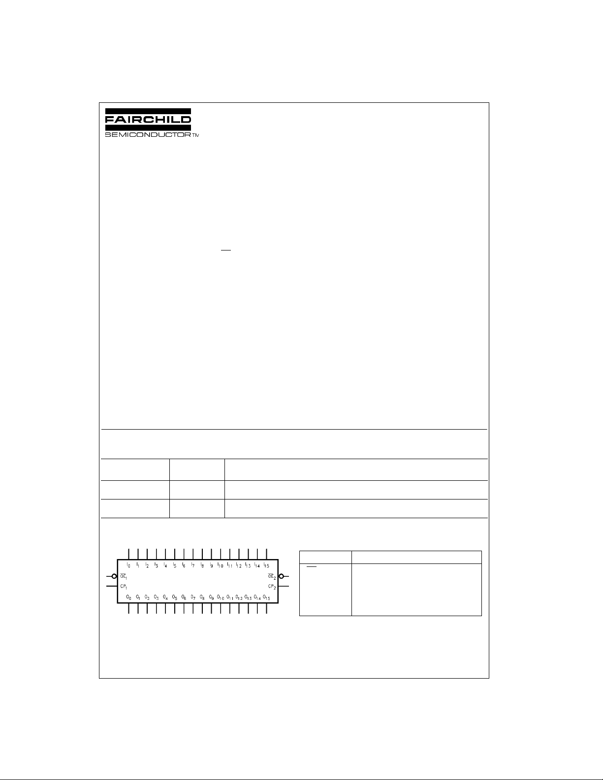
Logic Symbol Pin Descriptions
Pin Names Description
OE
n
CP
n
I
0–I15
O
0–O15
© 2000 Fairchild Semiconductor Corporation DS500226 www.fairchildsemi.com
Output Enable Input (Active LOW)
Clock Pulse Input
Bushold Inputs
Outputs
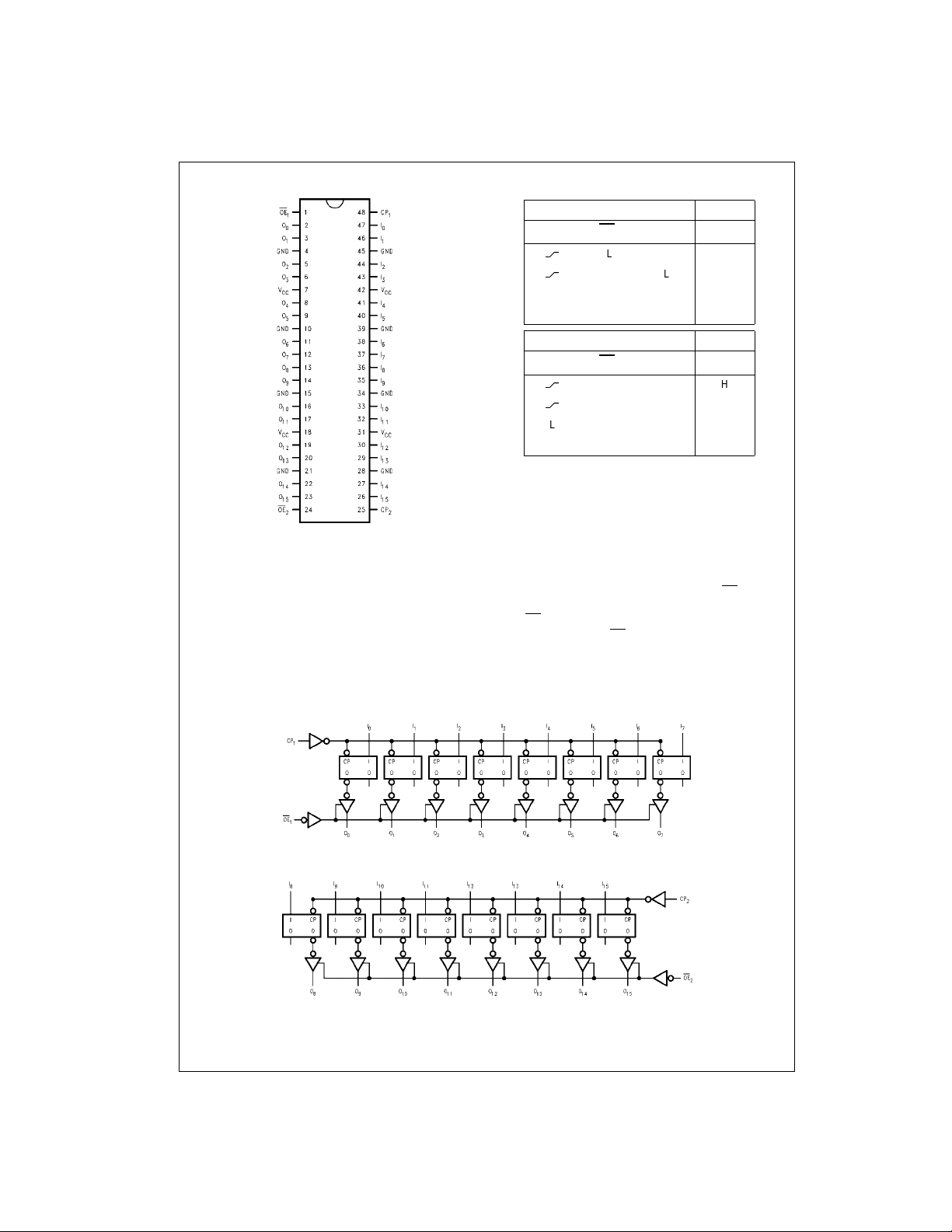
Connection Diagram Truth Tables
CP
74VCXH162374
CP
H = HIGH Voltage Level
L = LOW Voltage Level
X = Immaterial (HIG H or LOW, control inputs may not float )
Z = High Impedance
= Previous O0 before HIGH-to-LOW of CP
O
0
Functional Description
The 74VCXH162374 consists of sixteen edge-triggered
flip-flops with individual D-type inputs and 3-STATE true
outputs. The device is byte controlled with each byte functioning identically, but independent of the other. The control
pins can be shor ted tog eth er to ob tai n fu ll 16 -b i t o per atio n.
Each clock has a buffered clock and buffered Output
Enable common to all flip-flops within that byte. The
description which follows applies to each b yte. Each flip-
flop will store the state of their individual I inputs that meet
the setup and hold time requirements on the LOW-to-HIGH
Clock (CP
n
the contents of the flip-flops are available at th e outputs.
When OE
n
state. Operations of the OE
of the flip-flops.
Inputs Outputs
OE
1
LHH
LLL
LLXO
I0–I
1
O0–O
7
7
0
XHXZ
Inputs Outputs
OE
2
LHH
LLL
LLXO
I8–I
2
O8–O
15
15
0
XHXZ
) transition. With the Output Enable (OEn) LOW,
is HIGH, the outputs go to the high i mpedance
input does not affect the state
n
Logic Diagram
Byte 1 (0:7)
Byte 2 (8:15)
Please note that this diagram is provided o nly f or t he understanding of lo gic operations and shou ld not be used to estimate propagation delays.
www.fairchildsemi.com 2
Absolute Maximum Ratings(Note 2) Recommended Operating
Supply Voltage (VCC) −0.5V to +4.6V
DC Input Voltage (V
, CP
OE
n
– I
I
0
15
Output Voltage (V
)
I
n
−0.5V to 4.6V
−0.5V to VCC to 0.5V
)
O
Outputs 3-STATED −0.5V to +4.6V
Outputs Active (Note 3) −0.5V to V
DC Input Diode Current (I
< 0V −50 mA
V
I
DC Output Diode Current (I
< 0V −50 mA
V
O
> V
V
O
CC
)
IK
)
OK
+0.5V
CC
+50 mA
DC Output Source/Sink Current
) ±50 mA
(I
OH/IOL
or GND Current per
DC V
CC
Supply Pin (I
Storage Temperature Range (T
or GND) ±100 mA
CC
) −65°C to +150°C
STG
Conditions
Power Supply
Operating 1.65V to 3.6V
Data Retention Only 1.2V to 3.6V
Input Voltage −0.3V to V
Output Voltage (VO)
Output in Active States 0V to V
Output in “OFF” State 0.0V to 3.6V
Output Current in I
VCC = 3.0V to 3.6V ±12 mA
= 2.3V to 2.7V ±8 mA
V
CC
= 1.65V to 2.3V ±3 mA
V
CC
Free Air Operating Temperature (T
Minimum Input Edge Rate (∆t/∆V)
= 0.8V to 2.0V, VCC = 3.0V 10 ns/V
V
IN
Note 2: The Absolute Maximum Ratings are those values beyond which
the safety of the device cannot be guaranteed. The device should not be
operated at these limits. The parametric values defined in the Electrical
Characteristics tables are not guaranteed at the Absolute Maximum Rat-
ings. The “Recommended Operating Conditions” table will define the conditions for actual device operation.
Absolute Maximum Rating must be observed.
Note 3: I
O
Note 4: Floating or unused control inputs must be held HIG H or LOW.
(Note 4)
OH/IOL
) −40°C to +85°C
A
DC Electrical Characteristics (2.7V < VCC ≤ 3.6V)
V
Symbol Parameter Conditions
V
IH
V
IL
V
OH
V
OL
I
I
I
I(HOLD)
I
I(OD)
I
OZ
I
OFF
I
CC
∆I
Note 5: An external driver must source at least the specified current to switch from LOW-to-HIGH.
Note 6: An external dri ve r m us t s ink at least the specified cur rent to switch from HIGH -t o-LOW.
Note 7: Outputs disab led or 3-STATE only.
HIGH Level Input Voltage 2.7 − 3.6 2.0 V
LOW Level Input Voltage 2.7 − 3.6 0.8 V
HIGH Level Output Voltage IOH = −100 µA 2.7 − 3.6 VCC − 0.2 V
LOW Level Output Voltage IOL = 100 µA 2.7 − 3.6 0.2 V
Input Leakage Current Control Pins 0 ≤ VI ≤ 3.6V 2.7 − 3.6 ±5.0 µA
Bushold Input Minimum VIN = 0.8V 3.0 7 5
Drive Hold Current VIN = 2.0V 3.0 −75
Bushold Input Over-Drive (Note 5) 3.6 450
Current to Change State (Note 6) 3.6 −450
3-STATE Output Leakage 0 ≤ VO ≤ 3.6V
Power-OFF Leakage Current 0 ≤ (VO) ≤ 3.6V 0 10 µA
Quiescent Supply Current VI = VCC or GND 2.7 − 3.6 20 µA
Increase in ICC per Input VIH = VCC −0.6V 2.7 − 3.6 750 µA
CC
Data Pins VI = VCC or GND 2.7 − 3.6 ±5.0 µA
IOH = −6 mA 2.7 2.2 V
IOH = −8 mA 3.0 2.4 V
IOH = −12 mA 3.0 2.2 V
IOL = 6 mA 2.7 0.4 V
IOL = 8 mA 3.0 0.55 V
IOL = 12 mA 3.0 0.8 V
VI = VIH or V
VCC ≤ (VO) ≤ 3.6V (Note 7) 2.7 − 3.6 ±20 µA
IL
CC
(V)
2.7 − 3.6 ±10 µA
Min Max Units
74VCXH162374
CC
CC
µA
µA
3 www.fairchildsemi.com
 Loading...