Fairchild Semiconductor 74VCX86MX, 74VCX86MTCX, 74VCX86MTC, 74VCX86M Datasheet

© 1999 Fairchild Semiconductor Corporation ds500163 www.fairchildsemi.com
July 1999
Revised July 1999
74VCX86 Low Voltage Quad 2-Input Exclusive-OR Gate with 3.6V Tolerant Inputs and Outputs
74VCX86
Low Voltage Quad 2-Input Exclusive-OR Gate with
3.6V Tolerant Inputs and Outputs
General Description
The VCX86 contains four 2-inp ut exclu sive OR ga tes. This
product is designed for low voltage (1.65V to 3.6V) V
CC
applications with I/O compatibility up to 3.6V
The 74VCX86 is fabr icated w ith an adva nced CM OS tec h-
nology to achieve high-speed oper ation while maintaining
low CMOS power dissipation.
Features
■ 1.65V-3.6V VCC supply operation
■ 3.6V tolerant inputs and outputs
■ t
PD
3.0 ns max for 3.0V to 3.6V V
CC
3.9 ns max for 2.3V to 2.7V V
CC
7.8 ns max for 1.65V to 1.95V V
CC
■ Power-off high impedance inputs and outputs
■ Static Drive (I
OH/IOL
)
±24 mA @ 3.0V V
CC
±18 ma @ 2.3V V
CC
±6 mA @ 1.65V V
CC
■ Uses patented Quiet Series noise/EMI reduction
circuitry
■ Latchup performance exceeds 300 mA
■ ESD performance:
Human body model > 2000V
Machine model > 250V
Ordering Code:
Devices also availab le in Tape and Reel. Specify by appending th e s uffix let t er “X” to the ordering code.
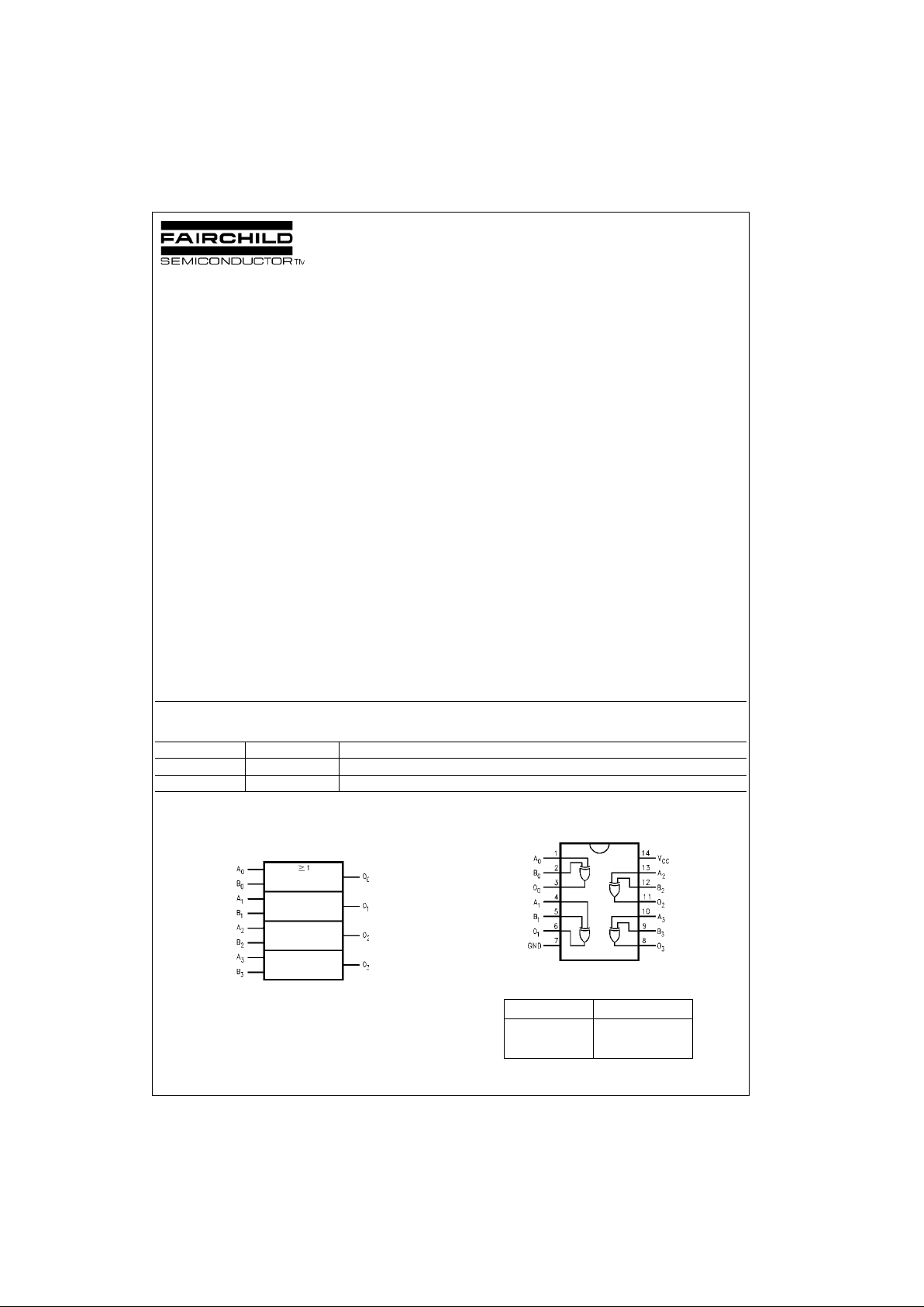
Logic Symbol
IEEE/IEC
Connection Diagram
Pin Descriptions
Quiet Series is a trademark of Fairchild Semiconductor Corporation
Order Number Package Number Package Description
74VCX86M M14A 14-Lead Small Outline Integrated Circuit (SOIC), JEDEC MS-120, 0.150” Narrow
74VCX86MTC MTC14 14-Lead Thin Shrink Small Outline Package (TSSOP), JEDEC MO-153, 4.4mm Wide
Pin Names Description
A
n
, B
n
Inputs
O
n
Outputs

www.fairchildsemi.com 2
74VCX86
Absolute Maximum Ratings(Note 1) Recommended Operating
Conditions
(Note 3)
Note 1: The Absolute Maximum Ratings are those values beyond which
the safety of the dev ice cannot be guaranteed. T he device sh ould not be
operated at these limits. The parametric values defined in the Electrical
Characteristics tables are not guaranteed at the Absolute Maximum Rat-
ings. The “Recommended Operating Conditions” table will define the conditions for actual device operation.
Note 2: I
O
Absolute Maximum Rating must be observed.
Note 3: Floating or unused inputs m us t be held HIGH or LOW
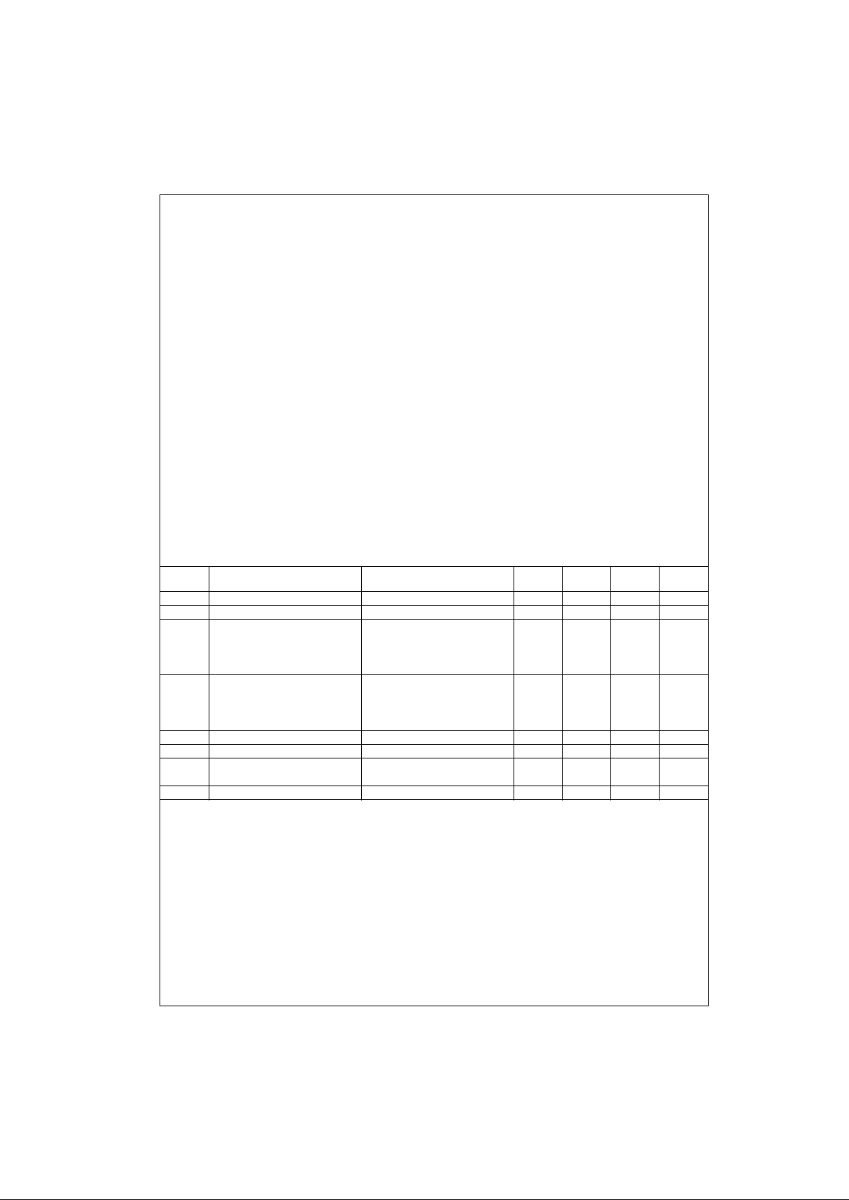
DC Electrical Characteristics (2.7V < VCC ≤ 3.6V)
Supply Voltage (VCC) −0.5V to +4.6V
DC Input Voltage (V
I
) −0.5V to +4.6V
Output Voltage (V
O
)
HIGH or LOW State (Note 2) −0.5V to V
CC
+0.5V
V
CC
= 0V −0.5V to +4.6V
DC Input Diode Current (I
IK
)
V
I
< 0V −50 mA
DC Output Diode Current (I
OK
)
V
O
< 0V −50 mA
V
O
> V
CC
+50 mA
DC Output Source/Sink Current (I
OH/IOL
) ±50 mA
DC V
CC
or Ground Current per ±100 mA
Supply Pin (I
CC
or Ground)
Storage Temperature Range (T
STG
) −65°C to +150°C
Power Supply
Operating 1.65V to 3.6V
Data Retention Only 1.2V to 3.6V
Input Voltage −0.3V to 3.6V
Output Voltage (V
O
)
HIGH or LOW State 0V to V
CC
Output Current in IOH/i
OL
VCC = 3.0V to 3.6V ±24 mA
V
CC
= 2.3V to 2.7V ±18 mA
V
CC
= 1.65V to 2.3V ±6 mA
Free Air Operating Temperature (T
A
) −40°C to +85°C
Minimum Input Edge Rate (∆t/∆V)
V
IN
= 0.8V to 2.0V, VCC = 3.0V 10 ns/V
Symbol Parameter Conditions
V
CC
(V)
Min Max Units
V
IH
HIGH Level Input Voltage 2.7–3.6 2.0 V
V
IL
LOW Level Input Voltage 2.7–3.6 0.8 V
V
OH
HIGH Level Output Voltage IOH = −100 µA 2.7–3.6 VCC − 0.2
V
IOH = −12 mA 2.7 2.2
IOH = −18 mA 3.0 2.4
IOH = −24 mA 3.0 2.2
V
OL
LOW Level Output Voltage IOL = 100 µA 2.7–3.6 0.2
V
IOL = 12 mA 2.7 0.4
IOL = 18 mA 3.0 0.4
IOL = 24 mA 3.0 0.55
I
I
Input Leakage Current 0 ≤ VI ≤ 3.6V 2.7–3.6 ±5.0 µA
I
OFF
Power-Off Leakage Current 0 ≤ (VI, VO) ≤ 3.6V 0 10 µA
I
CC
Quiescent Supply Current VI = VCC or GND 2.7–3.6 20
µA
VCC ≤ VI ≤ 3.6V 2.7–3.6 ±20
∆I
CC
Increase in ICC per Input VIH = VCC −0.6V 2.7–3.6 750 µA
 Loading...