Fairchild Semiconductor 74VCX32373 Datasheet

Preliminary
February 2001
Revised August 2001
74VCX32373
Low Voltage 32-Bit Transparent Latch
with 3.6V Tolerant Inputs and Outputs (Preliminary)
74VCX32373 Low Voltage 32-Bit Transparent Latch with 3.6V Tolerant Inputs and Outputs (Preliminary)
General Description
The VCX32373 contains thirty-two non-inverting latches
with 3-STATE outputs and is intended for bus oriented
applications. The device is byte controlled. The flip-flops
appear to be transparent to the data when the Latch enable
(LE) is HIGH. When LE is LOW, the data that meet s the
setup time is latched. Data appea rs on the bus when the
Output Enable (OE
puts are in a high impedance state.
The 74VCX32373 is designed for low voltage (1.65V to
3.6V) V
CC
The 74VCX32373 i s fabricated with an advanc ed CMOS
technology to achieve high speed operation while maintaining low CMOS power dissipation.
) is LOW. When OE is HIGH, the out-
applications with I/O compatibility up to 3.6V.
Features
■ 1.65V–3.6V VCC supply operation
■ 3.6V tolerant inputs and outputs
(In to On)
■ t
PD
3.0 ns max for 3.0V to 3.6V V
3.4 ns max for 2.3V to 2.7V V
6.8 ns max for 1.65V to 1.95V V
■ Power-off high impedance inputs and outputs
■ Support live insertion and withdrawal (Note 1)
■ Static Drive (I
±24 mA @ 3.0V V
±18 mA @ 2.3V V
±6 mA @ 1.65V V
■ Uses patented noise/EMI reductio n circuitr y
■ Latch-up performance exce eds 300 mA
■ ESD performance:
Human body model
Machine model
■ Packaged in plastic Fine-Pitch Ball Grid Array (FBGA)
Note 1: To ensure the high-impedance state d uring power up or power
should be tied to VCC through a pull-up r esistor; the min imum
down, OE
value of the res istor is d eter mine d by the cu rre nt-sou rcin g ca pa bility of t he
driver.
OH/IOL
)
CC
CC
CC
> 2000V
> 200V
Ordering Code:
Ordering Number Package Number Package Descript ion
74VCX32373GX
(Note 2)
Note 2: BGA package available in Tape and Reel only.
BGA96A 96-Ball Fine-Pitch Ball Grid Array (FBGA), JEDEC MO-205, 5.5mm Wide
[TAPE and REEL]
CC
CC
CC
Logic Symbol
© 2001 Fairchild Semiconductor Corporation DS500567 www.fairchildsemi.com

Preliminary
Connection Diagram
Pin Assignment for FBGA
74VCX32373
(Top Thru View)
Pin Descriptions
Pin Names Description
OE
LE
I
0–I31
O
0–O31
n
n
Output Enable Input (Active LOW)
Latch Enable Input
Inputs
Outputs
FBGA Pin Assignments
123456
A O
B O
C O
D O
E O
F O
G O
H O
J O
K O
L O
M O
N O
P O
R O
T O
O0OE1LE
1
O2GND GND I
3
O4V
5
7
9
11O10VCCVCCI10I11
13O12
14O15
17O16
19O18
21O20VCCVCCI20I21
23O22
25O24
27O26VCCVCCI26I27
29O28
30O31
CCVCCI4
O6GND GND I
O8GND GND I
GND GND I
OE2LE2I
OE3LE3I
GND GND I
GND GND I
GND GND I
GND GND I
OE4LE4I
1I0
2
6
8
12I13
15I14
16I17
18I19
22I23
24I25
28I29
31I30
I
1
I
3
I
5
I
7
I
9
Truth Tables
Inputs Outputs
LE
1
XHXZ
HLLL
HLHH
LLXO
LE
2
XHXZ
HLLL
HLHH
LLXO
H = HIGH Voltage Level
L = LOW Voltage Level
X = Immaterial (HIGH or LOW, inputs may not float)
www.fairchildsemi.com 2
OE
1
I0–I
7
O0–O
0
Inputs Outputs
OE
2
I8–I
15
O8–O
0
7
15
Inputs O utputs
LE
3
OE
3
I16–I
O16–O
23
XHXZ
HLLL
HLHH
LLXO
Inputs O utputs
LE
4
OE
4
I24–I
O24–O
31
XHXZ
HLLL
HLHH
LLXO
Z = High Impedance
= Previous O0 before HIGH-to-LOW of Latch Enable
O
0
23
0
31
0

Functional Description
The 74VCX32373 conta ins thirty-two edge D-typ e latches
with 3-STATE outputs. The dev ice is byte controlled with
each byte functioning identically, but independent of the
other. Control pins can be sh orted together to obtain full
32-bit operation. The foll owing description ap plies to each
byte. When the Latch Enable (LE
enters the latches. In this condit ion the latches are
the I
n
transparent, i.e., a latch output will change state each time
) input is HIGH, data on
n
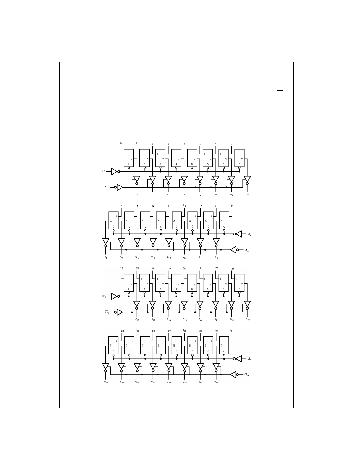
Logic Diagrams
Preliminary
its I input changes. When LE
information that was present on the I inputs a setup time
preceding the HIGH-to-LOW transition on LE
STATE o utputs are co ntrolled by the Output En able (OE
input. When OE
state mode. When OE
in the high impedance mode but this does not interfere with
entering new data into the latches.
is LOW the standard outputs are in the 2-
n
is LOW, the latches store
n
. The 3-
n
is HIGH, the standard outputs are
n
74VCX32373
)
n
Please note that this diagram is provided only for the understanding of logic operations and should not be used to estimate propagation delays.
3 www.fairchildsemi.com
 Loading...