

Fairchild Semiconductor 74VCX32245 Datasheet
Preliminary
August 2001
Revised August 2001
74VCX32245
Low Voltage 32-Bit Bidirectional Tr ans ceiver
with 3.6V Tolerant Inputs and Outputs (Preliminary)
74VCX32245 Low Voltage 32-Bit Bidirectional Transceiver with 3.6V Tolerant Inputs and Outputs (Preliminary)
General Description
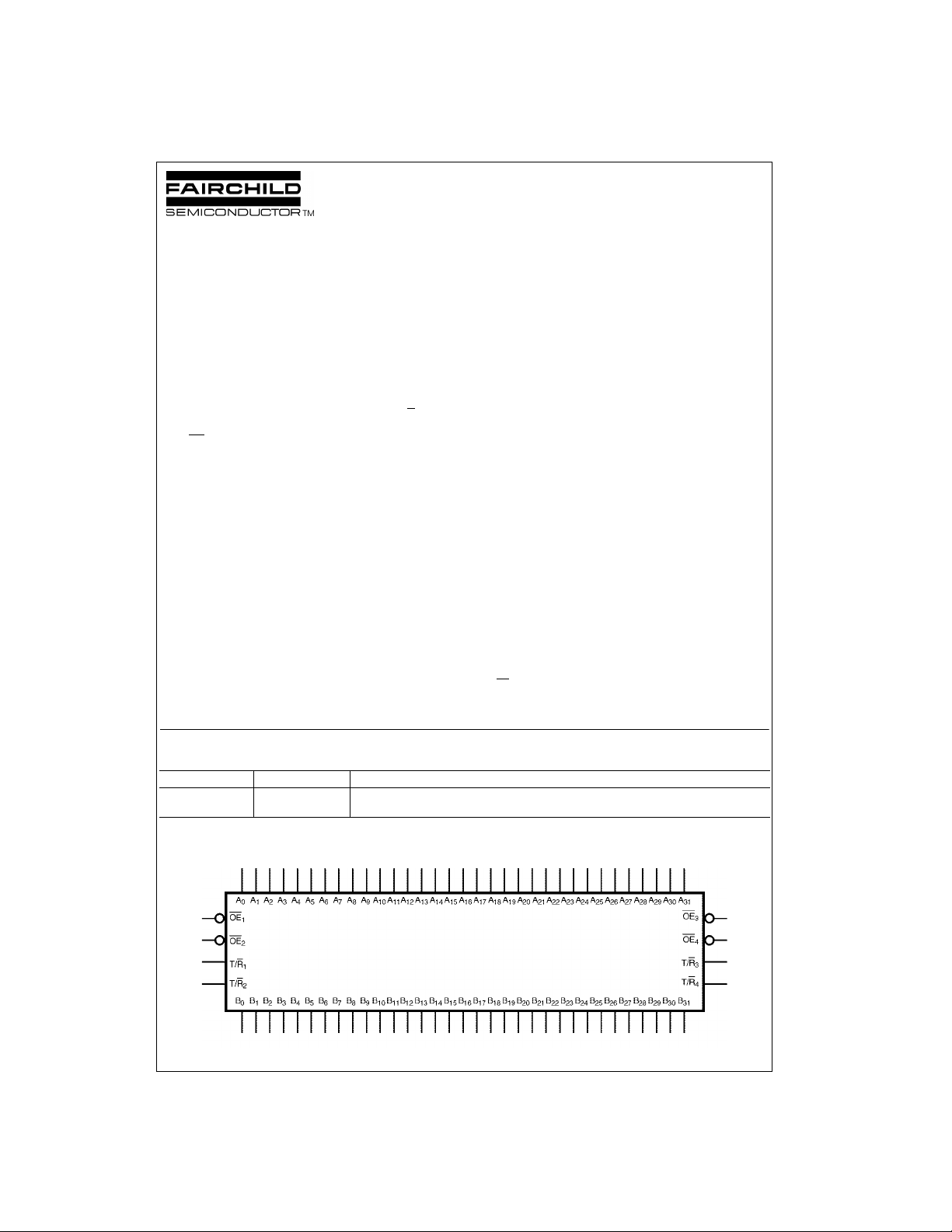
The VCX32245 contains thirty-two non-inverting bidirectional buffers with 3-STATE outputs and is intended for bus
oriented applications. The device is byte control led. Each
byte has separate 3-STATE control inputs which can be
shorted together for full 32-bit operation. Th e T/R
determine the dire ction of data flow through the device.
The OE
inputs disable bo th the A and B ports by placing
them in a high impedance state.
The 74VCX32245 is designed for low voltage (1.65V to
3.6V) V
The 74VCX32245 i s fabricated with an advanc ed CMOS
technology to achieve high speed operation while maintaining low CMOS power dissipation.
applications with I/O compatibility up to 3.6V.
CC
inputs
Features
■ 1.65V–3.6V VCC supply operation
■ 3.6V tolerant inputs and outputs
■ t
PD
2.5 ns max for 3.0V to 3.6V V
3.0 ns max for 2.3V to 2.7V V
6.0 ns max for 1.65V to 1.95V V
■ Power-down high impedance inputs and outputs
■ Supports live insertion/withdrawal (Note 1)
■ Static Drive (I
±24 mA @ 3.0V V
±18 mA @ 2.3V V
±6 mA @ 1.65V V
■ Uses patented noise/EMI reductio n circuitr y
■ Latchup performance exceeds 300 mA
■ ESD performance:
Human body model
Machine model
■ Packaged in plastic Fine-Pitch Ball Grid Array (FBGA)
Note 1: To ensure the high-impedance state d uring power up or power
should be tied to VCC through a pull-up r esistor; the min imum
down, OE
value of the res istor is d eter mine d by the cu rre nt-sou rcin g ca pa bility of t he
driver.
OH/IOL
)
CC
CC
>200V
Ordering Code:
Order Number Package Number Package Description
74VCX32245GX
(Note 2)
Note 2: BGA package available in Tape and Reel only.
BGA96A 96-Ball Fine-Pitch Ball Grid Array (FBGA), JEDEC MO-205, 5.5mm Wide
[Tape and Reel]
CC
CC
CC
CC
> 2000V
Logic Symbol
© 2001 Fairchild Semiconductor Corporation DS500415 www.fairchildsemi.com
Preliminary
Connection Diagram
74VCX32245
(Top Thru View)
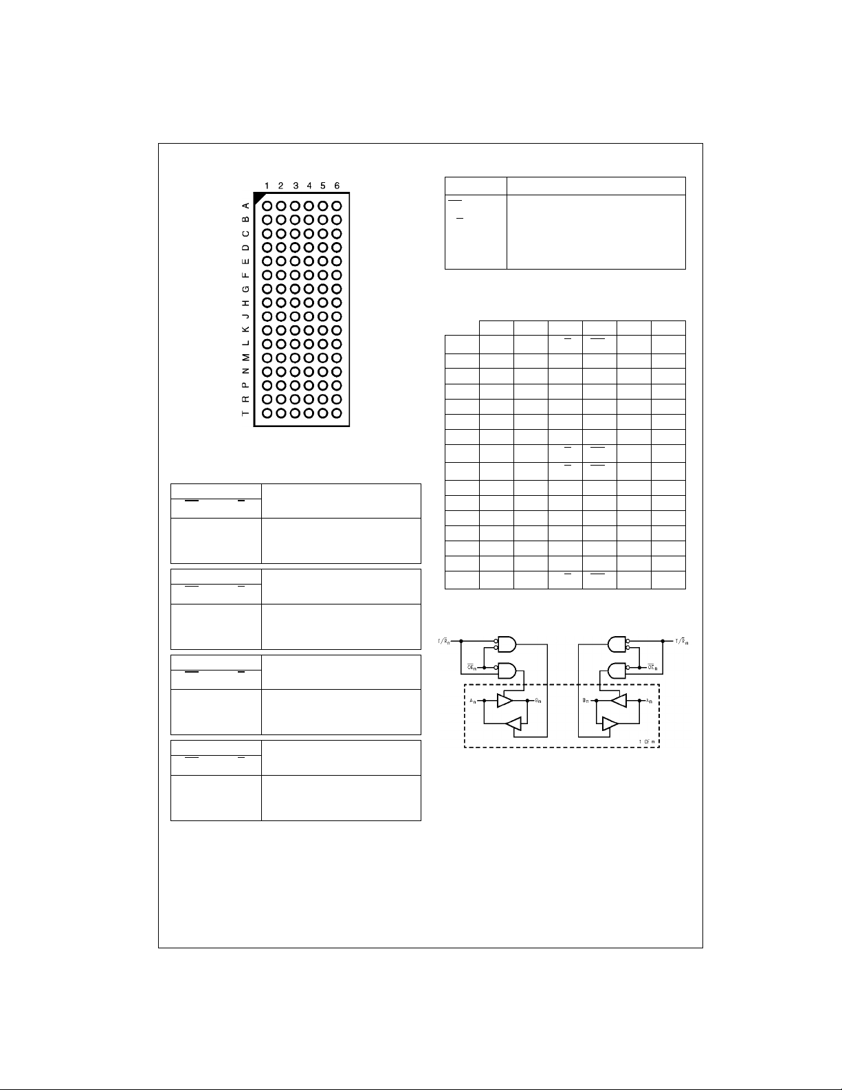
Truth Tables
Inputs
OE
T/R
1
1
L L Bus B0–B7 Data to Bus A0–A
L H Bus A0–A7 Data to Bus B0–B
H X HIGH Z State on A0–A7, B0–B
Inputs
OE
T/R
2
2
LLBus B
L H Bus A8–A15 Data to Bus B8–B
H X HIGH Z State on A8–A15, B8–B
Inputs
OE
T/R
3
3
L L Bus B16–B23 Data to Bus A16–A
L H Bus A16–A23 Data to Bus B16–B
H X HIGH Z State on A16–A23, B16–B
Inputs
OE
T/R
4
4
L L Bus B24–B31 Data to Bus A24–A
L H Bus A24–A31 Data to Bus B24–B
H X HIGH Z State on A24–A31, B24–B
H = HIGH Voltage Level
L = LOW Voltage Level
X = Immaterial (HIGH or LOW, inputs and I/O’s may not float)
Z = High Impedance
Outputs
Outputs
Data to Bus A8–A
8–B15
Outputs
Outputs
Pin Descriptions
Pin Names Description
OE
T/R
A
0–A31
B
0–B31
n
n
Output Enable Input (Active LOW)
Transmit/Receive Input
Side A Inputs or 3-STATE Outputs
Side B Inputs or 3-STATE Outputs
FBGA Pin Assignments
123456
A B
B B
C B
D B
E B
F B
G B13B12GND GND A12A
H B
J B17B16T/R3OE3A
K B
L B
7
7
7
M B23B22GND GND A22A
N B
P B
R B
T B
15
15
Logic Diagram
15
23
23
23
31
31
31
B0T/R1OE1A
1
B2GND GND A2A
3
B4V
5
7
9
11B10VCCVCCA10A11
14B15
19B18
21B20VCCVCCA20A21
25B24
27B26VCCVCCA26A27
29B28
30B31
CCVCCA4
B6GND GND A6A
B8GND GND A8A
T/R2OE2A
GND GND A18A
GND GND A24A
GND GND A28A
T/R4OE4A
A
0
A
15A14
16A17
31A30
1
3
5
7
9
13
19
23
25
29
www.fairchildsemi.com 2
Absolute Maximum Ratings(Note 3) Recommended Operating
Supply Voltage (VCC) −0.5V to +4.6V
DC Input Voltage (V
Output Voltage (V
Outputs 3-STATE
Outputs Active (Note 4)
DC Input Diode Current (I
DC Output Diode Current (I
V
< 0V −50 mA
O
V
> V
O
CC
) −0.5V to +4.6V
I
)
O
−0.5V to +4.6V
−0.5 to V
) VI < 0V −50 mA
IK
)
OK
CC
+50 mA
+ 0.5V
DC Output Source/Sink Current
) ±50 mA
(I
OH/IOL
DC V
or Ground Current per
CC
Supply Pin (I
Storage Temperature Range (T
or Ground) ±100 mA
CC
) −65°C to +150°C
STG
Conditions
Power Supply
Operating 1.65V to 3.6V
Data Retention Only 1.2V to 3.6V
Input Voltage
Output Voltage (V
Output in Active States 0V to V
Output in 3-STATE 0.0V to 3.6V
Output Current in I
VCC = 3.0V to 3.6V ±24 mA
= 2.3V to 2.7V ±18 mA
V
CC
V
= 1.65V to 2.3V ±6 mA
CC
Free Air Operating Temperature (T
Minimum Input Edge Rate (
V
= 0.8V to 2.0V, VCC = 3.0V 10 ns/V
IN
Note 3: The “Absolute Maximum Ratings” are those value s beyond which
the safety of the d evice cannot b e guaranteed . The device sh ould not be
operated at thes e limits. The param etric values define d in the “Electrical
Characteristics” table are not guaran teed at the Absolut e Maximum Ratings. The Recommended Operating C onditions tables will define the conditions for actual device oper ation.
Absolute Maximum Rating must be observed.
Note 4: I
O
Note 5: Floating or unused pi n (inputs or I/O's) must be held HIGH or LOW.
(Note 5)
)
O
OH/IOL
) −40°C to +85°C
A
∆t/∆V)
Preliminary
74VCX32245
−0.3V to 3.6V
CC
DC Electrical Characteristics (2.7V < V
Symbol Parameter Conditions
V
IH
V
IL
V
OH
V
OL
I
I
I
OZ
I
OFF
I
CC
∆I
Note 6: Outputs disabled or 3-STATE only.
HIGH Level Input Voltage 2.7–3.6 2.0 V
LOW Level Input Voltage 2.7–3.6 0.8 V
HIGH Level Output Voltage IOH = −100 µA2.7–3.6 VCC − 0.2
LOW Level Output Voltage IOL = 100 µA2.7–3.6 0.2
Input Leakage Current 0V ≤ VI ≤ 3.6V 2.7–3.6 ±5.0 µA
3-STATE Output Leakage 0V ≤ VO ≤ 3.6V
Power Off Leakage Current 0V ≤ (VI, VO) ≤ 3.6V 0 10 µA
Quiescent Supply Current VI = VCC or GND 2.7–3.6 40
Increase in ICC per Input VIH = VCC − 0.6V 2.7–3.6 750 µA
CC
I
= −12 mA 2.7 2.2
OH
= −18 mA 3.0 2.4
I
OH
IOH = −24 mA 3.0 2.2
= 12 mA 2.7 0.4
I
OL
IOL = 18 mA 3.0 0.4
I
= 24 mA 3.0 0.55
OL
VI = VIH or V
VCC ≤ (VI, VO) ≤ 3.6V (Note 6) 2.7–3.6 ±40
CC
IL
≤ 3.6V)
V
CC
(V)
2.7–3.6 ±10 µA
Min Max Units
V
V
µA
3 www.fairchildsemi.com
 Loading...