Fairchild Semiconductor 74VCX16722MTDX, 74VCX16722MTD Datasheet

© 2000 Fairchild Semiconductor Corporation DS500192 www.fairchildsemi.com
February 1999
Revised July 2000
74VCX16722 Low Voltage 22-Bit Register with 3.6V Tolerant Inputs and Outputs
74VCX16722
Low Voltage 22-Bit Register
with 3.6V Tolerant Inputs and Outputs
General Description
The VCX16722 low voltage 22- bit reg i ster conta ins twen tytwo non-inverting D-type flip-flops with 3-STATE outputs
and is intended for b us oriented applicati ons. The design
has been optimized for use wit h JEDE C compli ant 2 00 pin
DIMM modules.
The 74VCX16722 is designed for low voltage (1.65V to
3.6V) V
CC
applications with I/O capability up to 3.6V.
The 74VCX16722 i s fabricated with an advanc ed CMOS
technology to achieve high speed operation while maintaining low CMOS power dissipation.
Features
■ 1.65V–3.6V VCC specifications provided
■ 3.6V tolerant inputs and outputs
■ t
PD
(CLK to On)
3.6ns max for 3.0V to 3.6V V
CC
4.6ns max for 2.3V to 2.7V V
CC
9.2ns max for 1.65V to 1.95V V
CC
■ Power-down high impedance inputs and outputs
■ Supports live insertion/withdrawal (Note 1)
■ Meets JEDEC registered module speci fic at ions
■ Static Drive (I
OH/IOL
)
±24mA @ 3.0V
±18mA @ 2.3V
±6mA @ 1.65V
■ Latchup performance exceeds 300 mA
■ ESD performance:
Human body model
> 2000V
Machine model
>200V
Note 1: To ensure the high-impedance state d uring power up or power
down, OE
should be tied to VCC through a pull-up r esistor; the min imum
value of the resistor is dete rmined by the curren t sourcing capability of the
driver.
Ordering Code:
Devices also availab le in Tape and Reel. Specify by appending the s uffix let te r “X” to the ordering code.
Order Number Package Number Package Description
74VCX16722MTD MTD64 64-Lead Thin Shrink Small Outline Package (TSSOP), JEDEC MO-153, 6.1mm Wide

www.fairchildsemi.com 2
74VCX16722
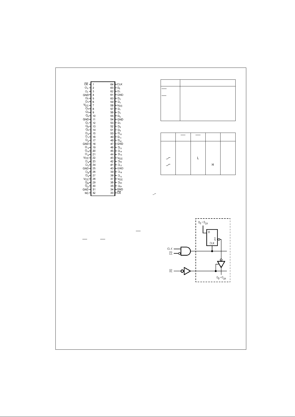
Connection Diagram Pin Descriptions
Tr uth Table
H = HIGH Voltage Level
L = LOW Level Voltage
X = Immaterial (HIGH or LOW, Inputs may not float)
Z = High Impedance
O0 = Previous O0 before L O W-to-HIG H transition of Clock
= LOW-to-HIGH transition
Functional Description
The VCX16722 contains twenty-two D-type flip-flops with
3-STATE standard outputs. The twenty-two flip-flops will
store the state of their indi vidual D-type inputs that meet
the setup and hold time requirements on the LOW-HIGH
Clock (CLK) transition, when the Clock-Enable (CE
) is
LOW. The 3-STATE standard outputs are cont rolle d by the
Output-Enable (OE
). When OE is HIGH, the standard outputs are in hi gh impedance mod e but this does not interfere with entering new data into the flip-flops.
Logic Diagram
Pin Names Description
OE
Output Enable Input (Active LOW)
CE
Clock Enable Input (Active Low)
CLK Clock Input
D
1
- D
21
Data Inputs
O
1
- O213-STATE Outputs
CLK CE
OE D0-D21O0-O
21
XXHXZ
XHLXO
0
LLLL
LLHH
L or H L L X O
0

3 www.fairchildsemi.com
74VCX16722
Absolute Maximum Ratings(Note 2) Recommended Operating
Conditions
(Note 4)
Note 2: The “Absolute Maximum Ratings” are those value s beyond which
the safety of the dev ice cannot b e guaranteed . The device sh ould not be
operated at these limit s. The parametric values defi ned in the Electrical
Characteristics tables are not guaranteed at the Absolute Maximum Ratings. The Recommended Operating Con ditions tables will define th e c onditions for actual device operat ion.
Note 3: I
O
Absolute Maximum Rating must be observed.
Note 4: Floating or unused pin (i nputs or I/O's) m ust be held HIGH o r LOW.
DC Electrical Characteristics (2.7V < VCC ≤ 3.6V)
Note 5: Outputs disabled or 3-STATE only.
Supply Voltage (VCC) −0.5V to +4.6V
DC Input Voltage (V
I
) −0.5V to +4.6V
Output Voltage (V
O
)
Outputs 3-STATE
−0.5V to +4.6V
Outputs Active (Note 3)
−0.5 to V
CC
+ 0.5V
DC Input Diode Current (I
IK
) VI < 0V −50 mA
DC Output Diode Current (I
OK
)
V
O
< 0V −50 mA
V
O
> V
CC
+50 mA
DC Output Source/Sink Current
(I
OH/IOL
) ±50 mA
DC V
CC
or Ground Current per
Supply Pin (I
CC
or Ground) ±100 mA
Storage Temperature Range (T
STG
) −65°C to +150°C
Power Supply
Operating 1.65V to 3.6V
Data Retention Only 1.2V to 3.6V
Input Voltage
−0.3V to 3.6V
Output Voltage (V
O
)
Output in Active States 0V to V
CC
Output in 3-STATE 0.0V to 3.6V
Output Current in I
OH/IOL
V
CC
= 3.0V to 3.6V ±24 mA
V
CC
= 2.3V to 2.7V ±18 mA
V
CC
= 1.65V to 2.3V ±6 mA
Free Air Operating Temperature (T
A
) −40°C to +85°C
Minimum Input Edge Rate (
∆t/∆V)
V
IN
= 0.8V to 2.0V, VCC = 3.0V 10 ns/V
Symbol Parameter Conditions
V
CC
Min Max Units
(V)
V
IH
HIGH Level Input Voltage 2.7–3.6 2.0 V
V
IL
LOW Level Input Voltage 2.7–3.6 0.8 V
V
OH
HIGH Level Output Voltage IOH = −100 µA2.7–3.6 VCC − 0.2
IOH = −12 mA 2.7 2.2
V
I
OH
= −18 mA 3.0 2.4
I
OH
= −24 mA 3.0 2.2
V
OL
LOW Level Output Voltage IOL = 100 µA2.7–3.6 0.2
I
OL
= 12 mA 2.7 0.4
V
I
OL
= 18 mA 3.0 0.4
IOL = 24 mA 3.0 0.55
I
I
Input Leakage Current 0V ≤ VI ≤ 3.6V 2.7–3.6 ±5.0 µA
I
OZ
3-STATE Output Leakage 0V ≤ VO ≤ 3.6V
2.7–3.6 ±10 µA
VI = VIH or V
IL
I
OFF
Power Off Leakage Current 0V ≤ (VI, VO) ≤ 3.6V 0 10 µA
I
CC
Quiescent Supply Current VI = VCC or GND 2.7–3.6 20
µA
VCC ≤ (VI, VO) ≤ 3.6V (Note 5) 2.7–3.6 ±20
∆I
CC
Increase in ICC per Input VIH = VCC − 0.6V 2.7–3.6 750 µA
 Loading...