Fairchild Semiconductor 74VCX132MX, 74VCX132MTCX, 74VCX132M Datasheet

© 1999 Fairchild Semiconductor Corporation ds500164 www.fairchildsemi.com
July 1999
Revised July 1999
74VCX132 Low Voltage Quad 2-Input NAND Gate with Schmitt Trigger Inputs and 3.6V Tolerant Inputs and Out-
puts
74VCX132
Low Voltage Quad 2-Input NAND Gate with
Schmitt Trigger Inputs and 3.6V Tolerant Inputs
and Outputs
General Description
The VCX132 contains four 2-input NAND gates with
Schmitt Trigger Inputs. The pin confi guration and function
are the same as the VCX00 except the inputs have hysteresis between the positive-go ing and negative-going input
thresholds. This hysteresis is useful for transforming slowly
switching input signals into sha rply defined, jitter-free output signals. This product should be used wher e n oise ma rgin greater than that of conventional gates is required.
The VCX132 is de signed for low voltage (1.6 5V to 3.6V)
V
CC
applications with I/O compatibility up to 3.6V.
This product is fabricated with an advanced CMOS technology to achieve high-speed oper ation while maintaining
low CMOS power dissipation.
Features
■ 1.65V-3.6V VCC supply operation
■ 3.6V tolerant inputs and outputs
■ t
PD
3.3 ns max for 3.0V to 3.6V V
CC
4.1 ns max for 2.3V to 2.7V V
CC
8.2 ns max for 1.65V to 1.95V V
CC
■ Power-off high impedance inputs and outputs
■ Static Drive (I
OH/IOL
)
±24 mA @ 3.0V V
CC
±18 mA @ 2.3V V
CC
±6 mA @ 1.65V V
CC
■ Uses patented Quiet Series noise/EMI reduction
circuitry
■ Latchup performance exceeds 300 mA
■ ESD performance:
Human body model > 2000V
Machine model > 250V
Ordering Code:
Devices also availab le in Tape and Reel. Specify by appending su ffix let te r “X” to the ordering code.
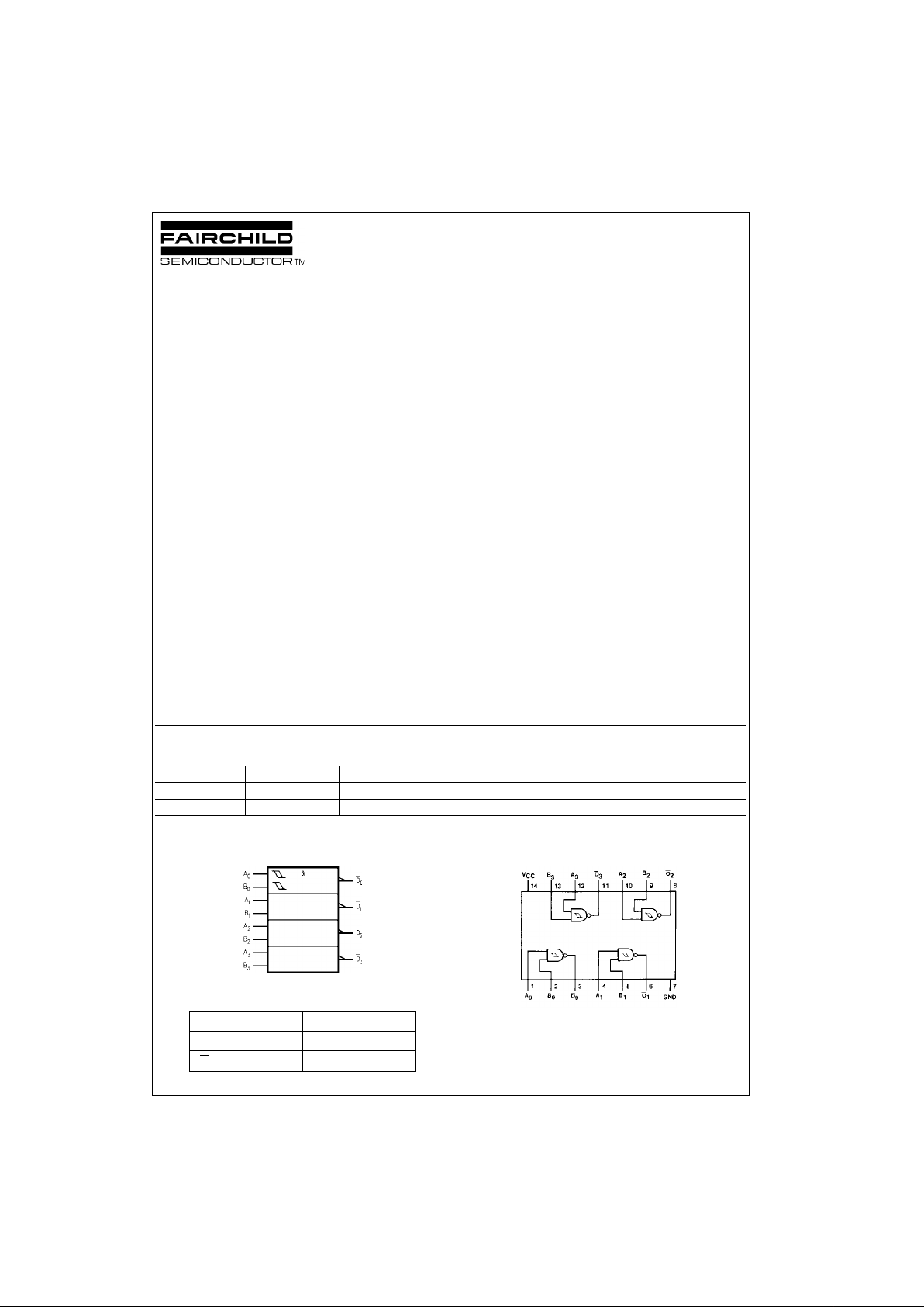
Logic Diagram
Pin Descriptions
Connection Diagram
Quiet Series is a trademark of Fairchild Semiconductor Corporation.
Order Number Package Number Package Description
74VCX132M M14A 14-Lead Small Outline Integrated Circuit (SOIC), JEDEC MS-120, 0.150” Narrow
74VCX132MTC MTC14 14-Lead Thin Shrink Small Outline Package (TSSOP), JEDEC MO-153, 4.4mm Wide
Pin Name Description
A
n
, B
n
Inputs
O
n
Outputs

www.fairchildsemi.com 2
74VCX132
Absolute Maximum Ratings(Note 1) Recommended Operating
Conditions
(Note 3)
Note 1: The “Absolute Maximum Ratin gs” are those v alues beyon d which
the safety of the dev ice cannot be guaranteed. T he device sh ould not be
operated at these limits. The parametric values defined in the Electrical
Characteristics tables are not guaranteed at the absolute maximum ratings.
The “Recommend ed O peratin g Cond itions” t able w ill defin e the co ndition s
for actual device operation.
Note 2: I
O
Absolute Maximum Rating must be observed.
Note 3: Floating or unused inputs m us t be held HIGH or LOW.
DC Electrical Characteristics (2.7V < VCC ≤ 3.6V)
Supply Voltage (VCC) −0.5V to +4.6V
DC Input Voltage (V
I
) −0.5V to 4.6V
DC Output Voltage (V
O
)
HIGH or LOW State (Note 2) −0.5V to V
CC
+ 0.5V
V
CC
= 0V −0.5V to +4.6V
DC Input Diode Current (I
IK
)
V
I
< 0V −50 mA
DC Output Diode Current (I
OK
)
V
O
< 0V −50 mA
V
O
> V
CC
+50 mA
DC Output Source/Sink Current ±50 mA
(I
OH/IOL
)
DC V
CC
or Ground Current per ±100 mA
Supply Pin (I
CC
or Ground)
Storage Temperature (T
STG
) −65°C to +150°C
Power Supply
Operating 1.65V to 3.6V
Data Retention Only 1.2V to 3.6V
Input Voltage −0.3V to 3.6V
Output Voltage (V
O
)
HIGH or LOW State 0V to V
CC
Output Current in IOH/I
OL
VCC = 3.0V to 3.6V ±24 mA
V
CC
= 2.3V to 2.7V ±18 mA
V
CC
= 1.65V to 2.3V ±6 mA
Free Air Operating Temperature (T
A
) −40°C to +85°C
Symbol Parameter Conditions
V
CC
(V)
Min Max Units
Vt+ Positive Threshold 3.6 2.2
V
3.0 2.0
Vt− Negative Threshold 3.6 0.8
V
3.0 0.7
V
H
Input Hysteresis 3.6 0.3 1.2
V
3.0 0.3 1.2
V
OH
HIGH Level Output Voltage IOH = −100 µA 2.7–3.6 VCC–0.2
V
IOH= −12 mA 2.7 2.2
IOH = −18 mA 3.0 2.4
IOH = −24mA 3.0 2.2
V
OL
LOW Level Output Voltage IOL = 100 µA 2.7–3.6 0.2
V
IOL = 12 µA2.70.4
IOL = 18 mA 3.0 0.4
IOL = 24 mA 3.0 0.55
I
I
Input Leakage Current 0 ≤ VI ≤ 3.6V 2.7–3.6 ±15.0 µA
I
OFF
Power Off Leakage Current 0 ≤ (VI, VO) ≤ 3.6V 0 10 µA
I
CC
Quiescent Supply Current VI = VCC or GND 2.7–3.6 20
µA
VCC ≤ VI ≤ 3.6V 2.7–3.6 ±20
∆I
CC
Increase in ICC per Input VIH = VCC – 0.6V 2.7–3.6 750 µA
 Loading...