Fairchild Semiconductor 74LVX574MTCX, 74LVX574MTC, 74LVX574M, 74LVX574SJX, 74LVX574SJ Datasheet
...
June 1993
Revised March 1999
74LVX574 Low Voltage Octal D-Type Flip-Flop with 3-STATE Outputs
© 1999 Fairchild Semiconductor Corporation DS500050.prf www.fairchildsemi.com
74LVX574
Low Voltage Octal D-Type Flip-Flop with
3-STATE Outputs
General Description
The LVX574 is a high-speed octal D-type flip-flop which is
controlled by an edge-triggered clock input (CP) and a buffered common Output Enable (OE
) input. When the OE
input is HIGH, the eight outputs are in a high im pedance
state. The LVX574 is functionally identical to the LVX374
but with inputs a nd outpu ts on op posite side s of t he pack-
age. The inputs tolerat e up to 7V allowing interface of 5V
systems to 3V systems.
Features
■ Input voltage translation from 5V to 3V
■ Ideal for low power/low noise 3.3V applications
■ Guaranteed simultaneous switching noise level and
dynamic threshold performance
Ordering Code:
Devices also availab le in Tape and Reel. Specify by appending th e s uffix let t er “X” to the ordering code.
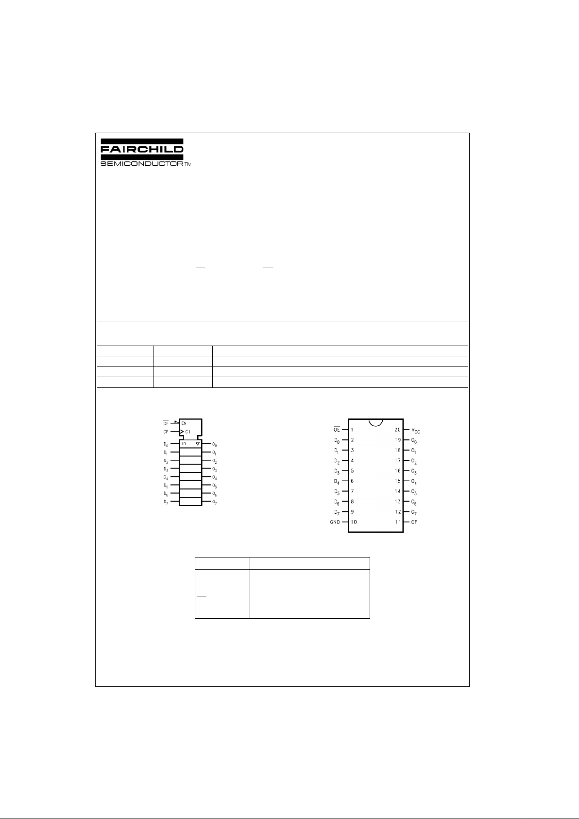
Logic Symbol Connection Diagram
Pin Descriptions
Order Number Package Number Package Description
74LVX574M M20B 20-Lead Small Outline Integrated Circuit (SOIC), JEDEC MS-013, 0.300” Wide
74LVX574SJ M20D 20-Lead Small Outline Package (SOP), EIAJ TYPE II, 5.3mm Wide
74LVX574MTC MTC20 20-Lead Thin Shrink Small Outline Package (TSSOP), JEDEC MO-153, 4.4mm Wide
Pin Names Description
D
0–D7
Data Inputs
CP Clock Pulse Input
OE
3-STATE Output Enable Input
O
0–O7
3-STATE Outputs

www.fairchildsemi.com 2
74LVX574
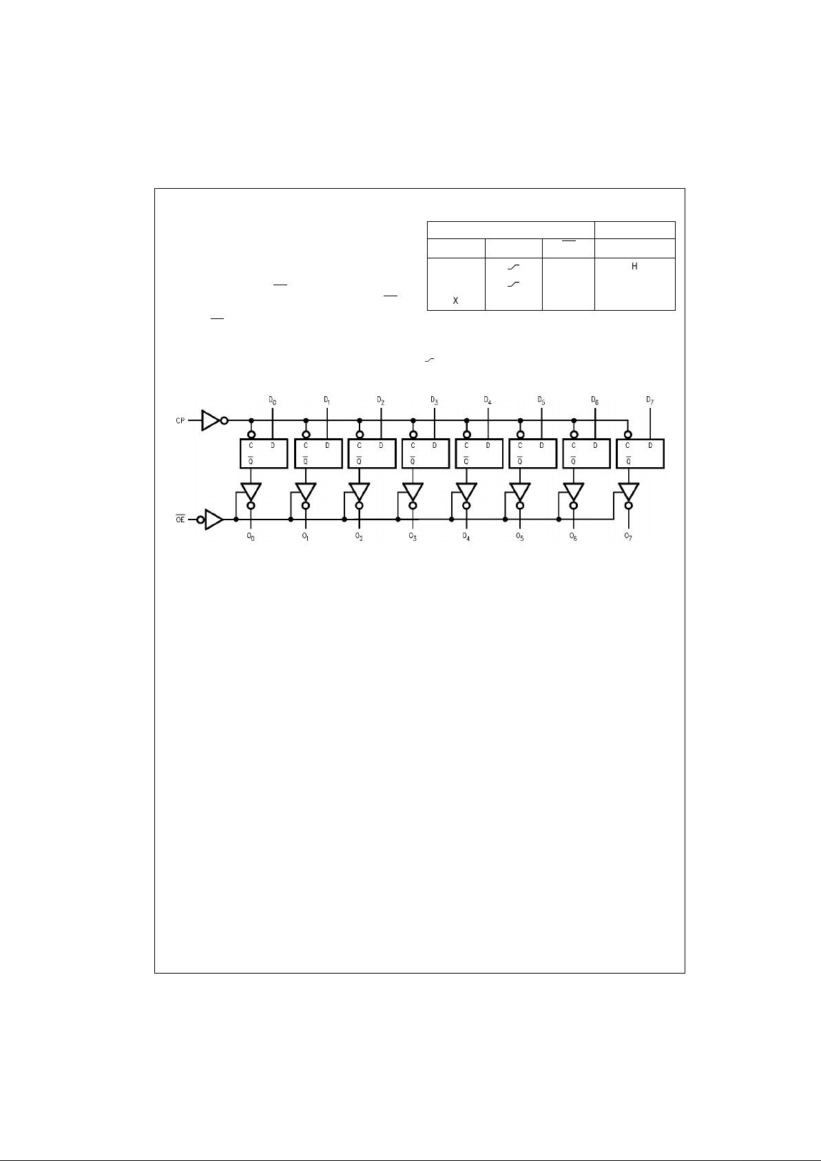
Functional Description
The LVX574 consists of eight e dge-tr iggere d flip -flops with
individual D-type inputs and 3-STATE true outputs. The
buffered clock and buffered Outp ut Enable are com mon to
all flip-flops. The eight flip-flops will store th e state of their
individual D inputs that meet the setup and hold time
requirements on the LOW-to-HIGH Clock (CP) transition.
With the Output Enable (OE
) LOW, the contents of the
eight flip-flops are available at the outputs. When the OE
is
HIGH, the outputs go to th e high impeda nce state. Op eration of the OE
input does not affect t he state of the flip-
flops.
Tr uth Table
H = HIGH Voltage Level
L = LOW Voltage Level
X = Immaterial
Z = High Impedance
= LOW-to-HIGH Transition
Logic Diagram
Please note that this diagram is provided only f or t he understanding of logic operations and should not be used to estimate propagation delays.
Inputs Outputs
D
n
CP OE O
n
H
LH
L
LL
XXH Z
 Loading...