Fairchild Semiconductor 74LVX573SJX, 74LVX573SJ, 74LVX573MX, 74LVX573MTCX, 74LVX573MTC Datasheet
...
June 1993
Revised March 1999
74LVX573 Low Voltage Octal Latch with 3-STATE Outputs
© 1999 Fairchild Semiconductor Corporation DS011616.prf www.fairchildsemi.com
74LVX573
Low Voltage Octal Latch with 3-STATE Outputs
General Description
The LVX573 is a high-speed octal latch with buff ered com mon Latch Enable (LE) and buffered common Output
Enable (OE
) inputs. The LVX573 is fu nct io na lly id entical to
the LVX373 but with inputs and outputs on opposite sides
of the package. The inp uts tole ra te u p to 7 V allo wing inte rface of 5V systems to 3V systems.
Features
■ Input voltage translation from 5V to 3V
■ Ideal for low power/low noise 3.3V applications
■ Guaranteed simultaneous switching noise level and
dynamic threshold performance
Ordering Code:
Devices also availab le in Tape and Reel. Specify by appending su ffix let te r “X” to the ordering code.
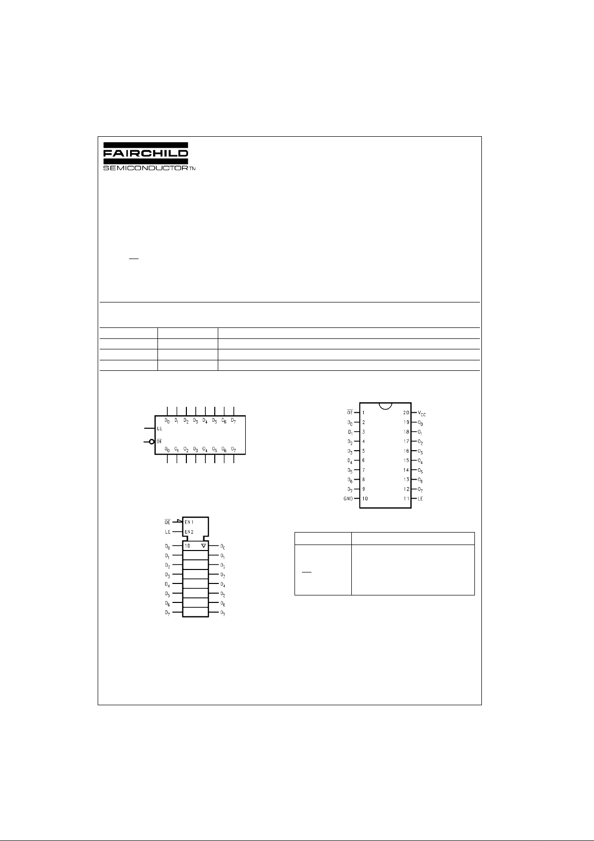
Logic Symbols
IEEE/IEC
Connection Diagram
Pin Descriptions
Order Number Package Number Package Description
74LVX573M M20B 20-Lead Small Outline Integrated Circuit (SOIC), JEDEC MS-013, 0.300” Wide
74LVX573SJ M20D 20-Lead Small Outline Package (SOP), EIAJ TYPE II, 5.3mm Wide
74LVX573MTC MTC20 20-Lead Thin Shrink Small Outline Package (TSSOP), JEDEC MO-153, 4.4mm Wide
Pin Names Description
D
0–D7
Data Inputs
LE Latch Enable Input
OE
3-STATE Output Enable Input
O
0–O7
3-STATE Latch Outputs

www.fairchildsemi.com 2
74LVX573
Functional Description
The LVX573 contains eight D-type latches. When the
enable (LE) input is HIGH, data on the D
n
inputs enters the
latches. In this condition the latches are transpar ent, i.e., a
latch output will change state each time its D input
changes. When LE is LOW the la tches store the information that was pres ent on th e D inp uts a s etup ti me preced ing the HIGH-to-LOW transition of LE. The 3-STATE
buffers are controlled by the Output Enable (OE
) input.
When OE
is LOW, the buffers are enabled. When OE is
HIGH the buffers are in the high imp edance mode but this
does not interfere with entering new data into the latches.
Tr uth Table
H = HIGH Voltage
L = LOW Voltage
Z = High Impedance
X = Immaterial
O0 = Previous O0 before HIGH-to-LOW transition of Lat ch Enable
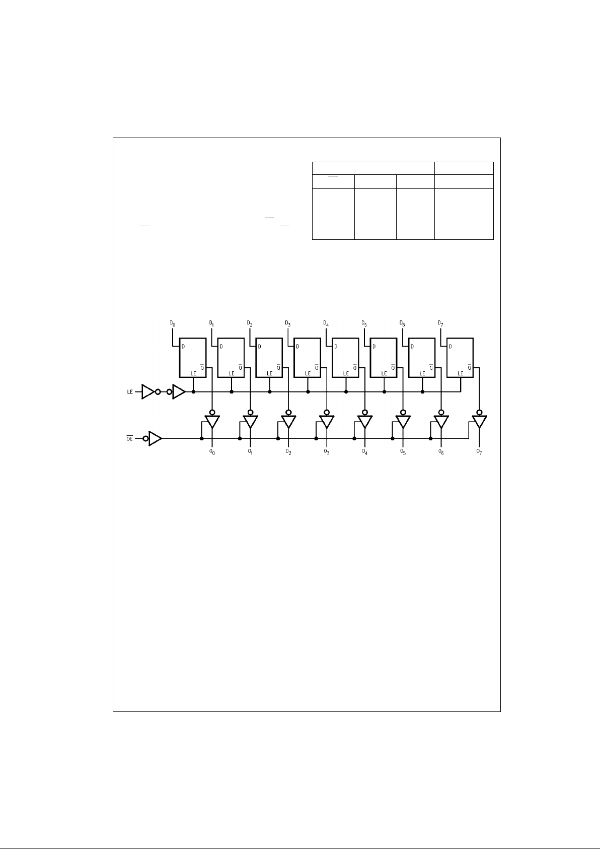
Logic Diagram
Please note that this diagram is provided o nly f or t he understanding o f lo gic operations and shou ld not be used to estimate propagation delays.
Inputs Outputs
OE
LE D O
n
LHH H
LHL L
LLX O
0
HXX Z
 Loading...