Fairchild Semiconductor 74LVX541SJX, 74LVX541SJ, 74LVX541MX, 74LVX541MTCX, 74LVX541MTC Datasheet
...
74LVX541
Low Voltage Octal Buffer/Line Dri ver with
3-STATE Outputs
74LVX541 Low Voltage Octal Buffer/Line Driver with 3-STATE Outputs
September 1999
Revised September 1999
General Description
The LVX541 is an octal non-i nver ting bu ffer an d line driv er
designed to be employed as a memory address driver,
clock driver and bus or iented transmitter or receive r which
provides improved PC board density. The inputs tolerate
up to 7V allowing interface of 5V systems to 3V systems.
Features
■ Input voltage translation from 5V to 3V
■ Ideal for low power/low noise 3.3V applications
■ Guaranteed simultaneous switching noise level and
dynamic threshold performance
Ordering Code:
Order Number Package Number Package Description
74LVX541M M20B 20-Lead Small Outline Integrated Circuit (SOIC), JEDEC MS-013, 0.300 Wide
74LVX541SJ M20D 20-Lead Small Outline Package (SOP), EIAJ TYPE II, 5.3mm Wide
74LVX541MTC MTC20 20-Lead Thin Shrink Small Outline Package (TSSOP), JEDEC MO-153, 4.4mm Wide
Surface mount pack ages are also available on Tape and Reel. Specify by appending the s uffix let te r “X” to the ordering code.
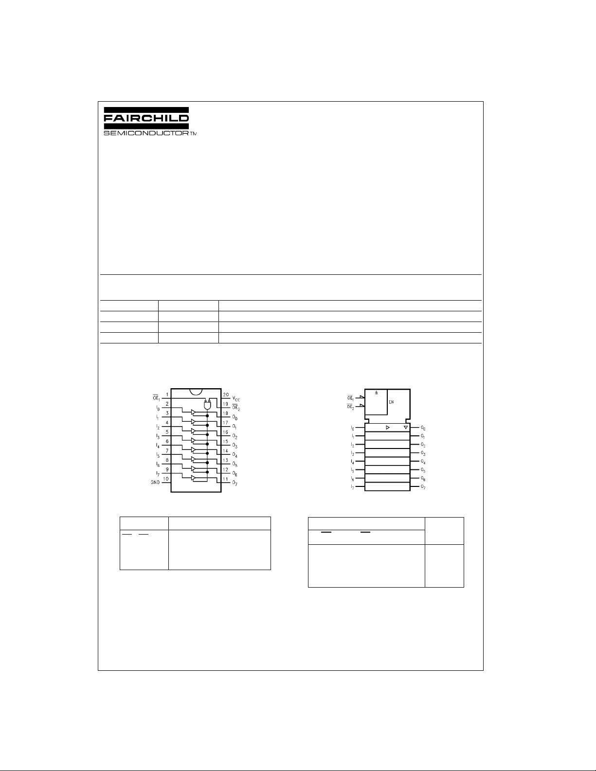
Connection Diagram
Logic Symbol
IEEE/IEC
Pin Descriptions
Pin Names Descriptions
, OE
OE
1
- I
I
0
7
- O
O
0
© 1999 Fairchild Semiconductor Corporation DS500291 www.fairchildsemi.com
3-STATE Output Enable Inputs
2
Inputs
3-STATE Outputs
7
Truth Table
Inputs
OE
1
LLHH
HXXZ
XHXZ
LLLL
H = HIGH Voltage Level X = Immaterial
L = LOW Voltage Level Z = High Impedance
OE
2
Outputs
I

Absolute Maximum Ratings(Note 1) Recommended Operating
Supply Voltage (VCC) −0.5V to +7.0V
DC Input Diode Current (I
74LVX541
= −0.5V −20 mA
V
I
DC Input Voltage (V
DC Output Diode Current (I
V
= −0.5V −20 mA
O
= VCC + 0.5V +20 mA
V
O
DC Output Voltage (V
)
IK
) −0.5V to 7V
I
)
OK
) −0.5V to VCC + 0.5V
O
DC Output Source
or Sink Current (I
or Ground Current
DC V
CC
(I
or I
CC
GND
Storage Temperature (T
) ±25 mA
O
) ±75 mA
) −65°C to +150°C
STG
Power Dissipation 180 mW
Conditions
Supply Voltage (V
Input Voltage (V
Output Voltage (V
Operating Temperature (TA) −40°C to +85°C
Input Rise and Fall Time (∆t/∆V) 0 ns/V to 100 ns/V
Note 1: The “Absolute Maximum Ratin gs” are those v alues beyon d which
the safety of the dev ice cannot be guaranteed. T he device sh ould not be
operated at these limits. The parametric values defined in the Electrical
Characteristics tables are not guaranteed at the absolute maximum ratings.
The “Recommend ed O peratin g Cond itions” t able w ill defin e the c ondit ions
for actual device operation.
Note 2: Unused inputs must be held HIGH or LOW. They may not float
(Note 2)
) 2.0V to +3.6V
CC
)0V to +5.5V
I
) 0V to V
O
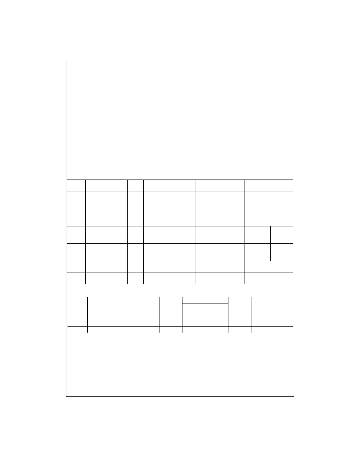
DC Electrical Characteristics
CC
Symbol Parameter
V
V
V
V
I
OZ
I
IN
I
CC
HIGH Level Input 2.0 1.5 1.5
IH
LOW Level Input 2.0 0.5 0.5
IL
HIGH Level Output 2.0 1.9 2.0 1.9 IOH = −50 µA
OH
Voltage 3.0 2.9 3.0 2.9 V VIN = VIH or VILIOH = −50 µA
LOW Level Output 2.0 0.0 0.1 0.1 IOL = 50 µA
OL
Voltage 3.0 0.0 0.1 0.1 V VIN = VIH or VILIOL = 50 µA
3-STATE Output
OFF-State Current V
Input Leakage Current 3.6 ±0.1 ±1.0 µAVIN = 5.5V or GND
Quiescent Supply Current 3.6 4.0 40.0 µAVIN = VCC or GND
Noise Characteristics
Symbol Parameter
V
OLP
V
OLV
V
IHD
V
ILD
Note 3: Input tr = tf = 3 ns.
Quiet Output Maximum Dynamic V
Quiet Output Minimum Dynamic V
Minimum HIGH Level Dynamic Input Voltage 3.3 2.0 V CL = 50 pF
Maximum HIGH Level Dynamic Input Voltage 3.3 0.8 V CL = 50 pF
V
CC
3.6 2.4 2.4
3.6 0.8 0.8
3.0 2.58 2.48 IOH = −4 mA
3.0 0.36 0.44 IOL = 4 mA
3.6 ±0.25 ±2.5 µA
TA = 25°CT
Min Typ Max Min Max
= −40°C to +85°C
A
Units Conditions
VVoltage 3.0 2.0 2.0
VVoltage 3.0 0.8 0.8
VIN = VIH or V
OUT
IL
= VCC or GND
(Note 3)
V
CC
(V)
OL
OL
3.3 0.5 0.8 V CL = 50 pF
3.3 −0.5 −0.8 V CL = 50 pF
TA = 25°C
Typ Limits
Units Conditions
www.fairchildsemi.com 2
 Loading...