Fairchild Semiconductor 74LVX373SJX, 74LVX373SJ, 74LVX373MX, 74LVX373MTCX, 74LVX373MTC Datasheet
...
June 1993
Revised March 1999
74LVX373 Low Voltage Octal Transparent Latch with 3-STATE Outputs
© 1999 Fairchild Semiconductor Corporation DS011613.prf www.fairchildsemi.com
74LVX373
Low Voltage Octal Transparent Latch with
3-STATE Outputs
General Description
The LVX373 consists of eight latches with 3-STATE outputs
for bus organized system applications. The latch es appe ar
transparent to the data when Latch Enable (LE) is HIGH.
When LE is LOW, the data satisfying the input timing
requirements is latched. Data appears on the bus when the
Output Enable (OE
) is LOW. When OE is HIGH, the bus
output is in the high impedance state. The inputs tolerate
up to 7V allowing interface of 5V systems to 3V systems.
Features
■ Input voltage translation from 5V to 3V
■ Ideal for low power/low noise 3.3V applications
Ordering Code:
Devices also availab le in Tape and Reel. Specify by appending su ffix let te r “X” to the ordering code.
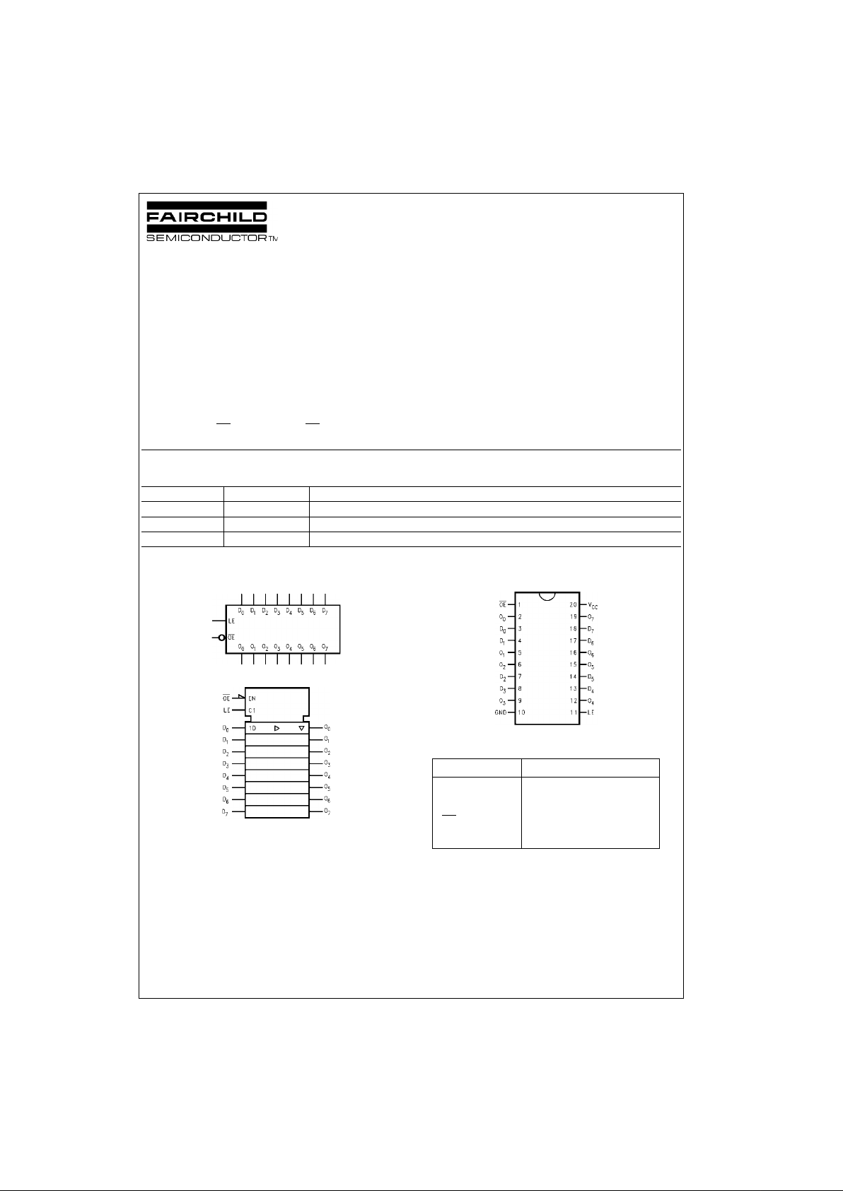
Logic Symbols
IEEE/IEC
Connection Diagram
Pin Descriptions
Order Number Package Number Package Description
74LVX373M M20B 20-Lead Small Outline Integrated Circuit (SOIC), JEDEC MS-013, 0.300” Wide
74LVX373SJ M20D 20-Lead Small Outline Package (SOP), EIAJ TYPE II, 5.3mm Wide
74LVX373MTC MTC20 20-Lead Thin Shrink Small Outline Package (TSSOP), JEDEC MO-153, 4.4mm Wide
Pin Names Description
D
0–D7
Data Inputs
LE Latch Enable Input
OE
Output Enable Input
O
0–O7
3-STATE Latch Outputs

www.fairchildsemi.com 2
74LVX373
Functional Description
The LVX373 contains eight D-type latches with 3-STATE
standard outputs. When the Latch Enable (LE) input is
HIGH, data on the D
n
inputs enters the latches. In this con-
dition the latches are transparent, i.e., a latch o utput will
change state each time its D input cha nges. When LE is
LOW, the latches store the information that was present on
the D inputs a setup time preceding the HIGH-to-LOW transition of LE. The 3-STATE standard outputs are controlle d
by the Output Enable (OE
) input. When OE is LOW, the
standard outputs are in the 2-state mode. When OE
is
HIGH, the standard outputs are in the high impedance
mode but this does not interfere with entering new data into
the latches.
Tr uth Table
H = HIGH Voltage Level
L = LOW Voltage Level
Z = High Impedance
X = Immaterial
O0 = Previous O0 before HIGH-to-LOW transition of Latch Enable
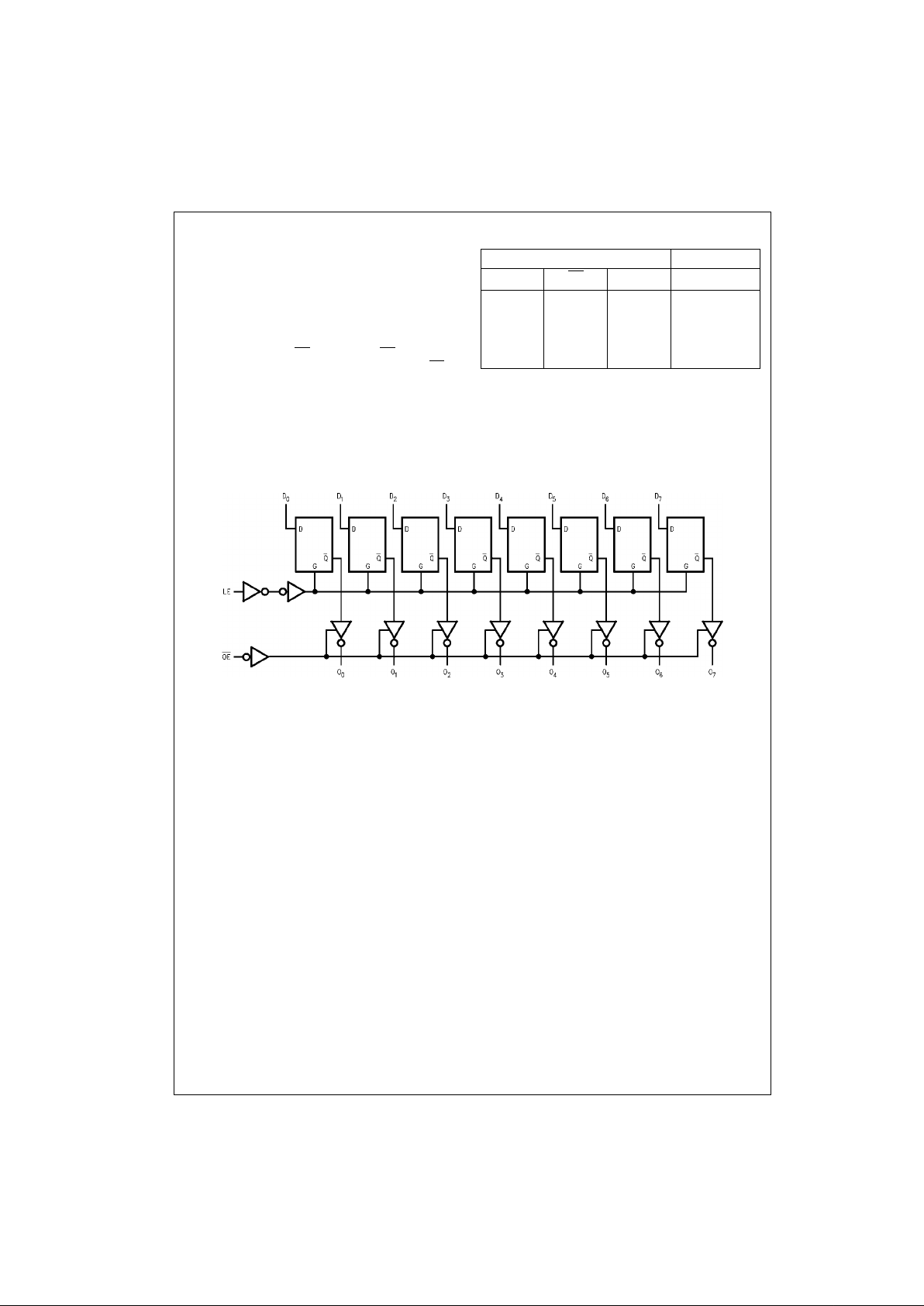
Logic Diagram
Please note that this diagram is provided o nly f or t he understanding of lo gic operations and should not be used to estimate propagation delays.
Inputs Outputs
LE OE
D
n
O
n
XHX Z
HLL L
HLH H
LLX O
0
 Loading...