Fairchild Semiconductor 74LVX3245MTCX, 74LVX3245WMX, 74LVX3245WM, 74LVX3245QSCX, 74LVX3245QSC Datasheet

© 1999 Fairchild Semiconductor Corporation DS011620 www.fairchildsemi.com
July 1993
Revised July 1999
74LVX3245 8-Bit Dual Supply Translating Transceiver with 3-STATE Outputs
74LVX3245
8-Bit Dual Supply Translating Transceiver with
3-STATE Outputs
General Description
The LVX3245 is a dual-supply, 8-bit tran slating transcei ver
that is designed to interface be tween a 3V bus and a 5V
bus in a mixed 3V/5V sup ply environment. The Transmit/
Receive (T/R
) input determines the direction of da ta flow.
Transmit (active-HIGH) enables data from A Ports to B
Ports; Receive (acti ve-LOW) en ables data from B Ports to
A Ports. The Output Enable input, w hen HIGH, disables
both A and B Ports by placing them in a h igh impedance
condition. The A Port interfaces with the 3V bus; the B Port
interfaces with the 5V bus.
The LVX3245 is suitable for mixed voltage applications
such as notebook computers using 3.3V CPU and 5V
peripheral components.
Features
■ Bidirectional interface between 3V and 5V buses
■ Inputs compatible with TTL level
■ 3V data flow at A Port and 5V data flow at B Port
■ Outputs source/sink 24 mA
■ Guaranteed simultaneous switching noise level and
dynamic threshold performance
■ Implements proprietary EMI reduction circuitry
■ Functionally compatible with the 74 series 245
Ordering Code:
Devices also availab le in Tape and Reel. Specify by appending su ffix let te r “X” to the ordering code .
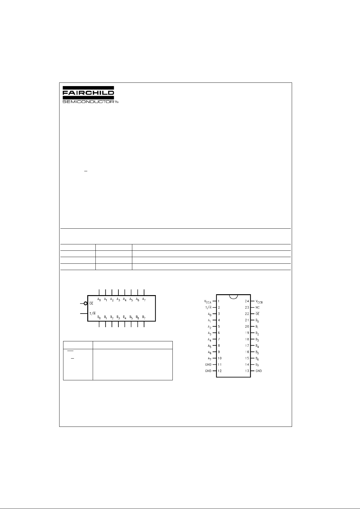
Logic Symbol
Pin Descriptions
Connection Diagram
Order Number Package Number Package Description
74LVX3245WM M24B 24-Lead Small Outline Integrated Circuit (SOIC), JEDEC MS-013, 0.300” Wide
74LVX3245QSC MQA24 24-Lead Quarter Size Outline Package (QSOP), JEDEC MO-137, 0.150” Wide
74LVX3245MTC MTC24 24-Lead Thin Shrink Small Outline Package (TSSOP), JEDEC MO-153, 4.4mm Wide
Pin Names Description
OE
Output Enable Input
T/R
Transmit/Receive Input
A
0–A7
Side A Inputs or 3-STATE Outputs
B
0–B7
Side B Inputs or 3-STATE Outputs

www.fairchildsemi.com 2
74LVX3245
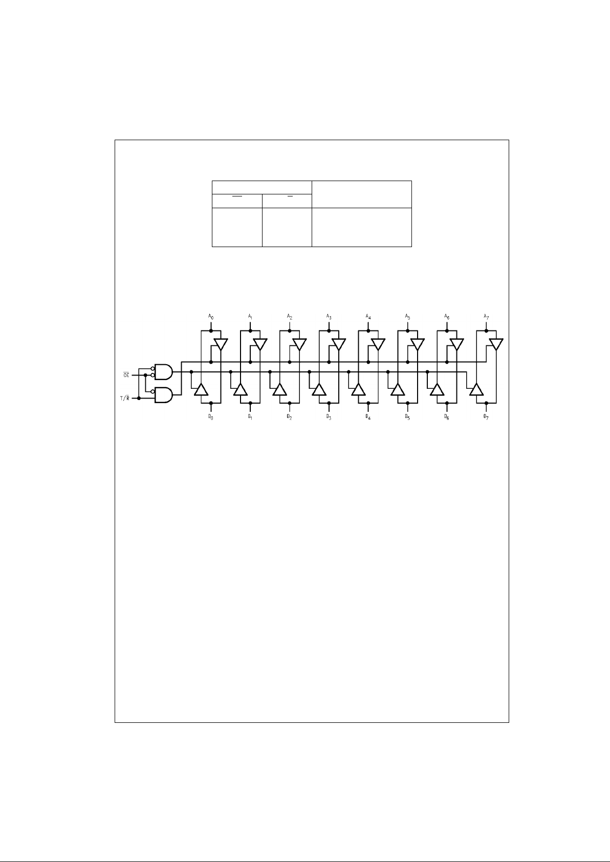
Truth Table
H = HIGH Voltage Level
L = LOW Voltage Level
X = Immaterial
Logic Diagram
Inputs Outputs
OE
T/R
L L Bus B Data to Bus A
L H Bus A Data to Bus B
H X HIGH-Z State

3 www.fairchildsemi.com
74LVX3245
Absolute Maximum Ratings(Note 1) Recommended Operating
Conditions
(Note 2)
Note 1: The “Absolute Maximum Ratings ” are those val ues beyond w hich
the safety of the device cannot be guaranteed. The device should not be
operated at these limits. The parametric values defined in the Electrical
Characteristics tables are not guaranteed at the absolute maximum ratings.
The “Recommend ed O peratin g Cond itions” t able w ill defin e the condition s
for actual device operation.
Note 2: Unused Pins (inputs an d I/Os) mu st be held H IGH or LOW. They
may not float.
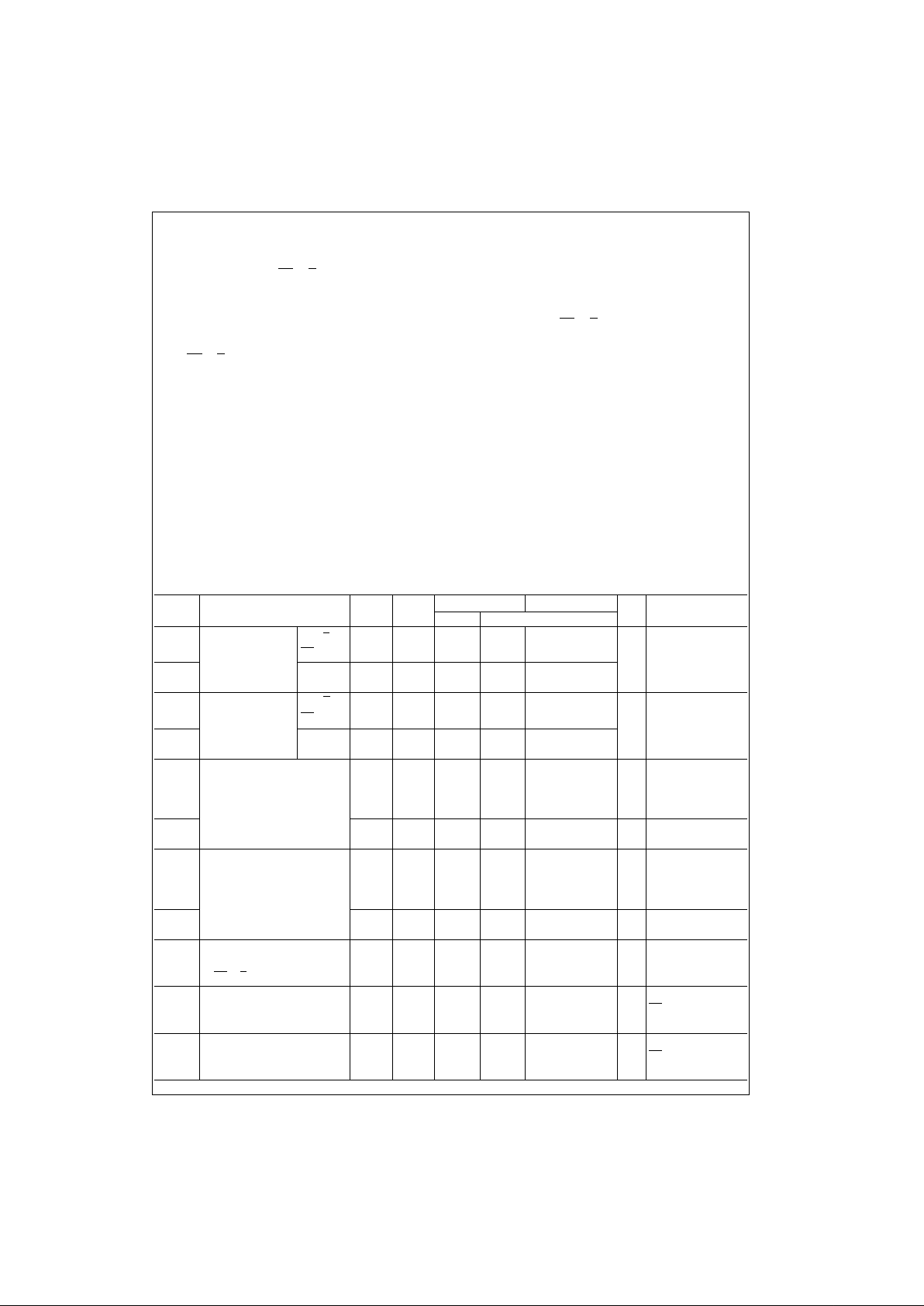
DC Electrical Characteristics
Supply Voltage (V
CCA
, V
CCB
) −0.5V to +7.0V
DC Input Voltage (V
I
) @ OE, T/R −0.5V to V
CCA
+ 0.5V
DC Input/Output Voltage (V
I/O
)
@ A
n
−0.5V to V
CCA
+ 0.5V
@ B
n
−0.5V to V
CCB
+ 0.5V
DC Input Diode Current (I
IN
)
@ OE
, T/R ±20 mA
DC Output Diode Current (I
OK
) ±50 mA
DC Output Source or
Sink Current (I
O
) ±50 mA
DC V
CC
or Ground Current
per Output Pin (I
CC
or I
GND
) ±50 mA
and Max Current @ I
CCA
±100 mA
@ I
CCB
±200 mA
Storage Temperature Range (T
STG
) −65°C to +150°C
DC Latch-Up Source or
Sink Current ±300 mA
Supply Voltage
V
CCA
2.7V to 3.6V
V
CCB
4.5V to 5.5V
Input Voltage (V
I
) @ OE, T/R 0V to V
CCA
Input/Output Voltage (V
I/O
)
@ A
n
0V to V
CCA
@ B
n
0V to V
CCB
Free Air Operating Temperature (TA) −40°C to +85°C
Minimum Input Edge Rate (∆t/∆V) 8 ns/V
V
IN
from 30% to 70% of V
CC
VCC @ 3.0V, 4.5V, 5.5V
Symbol Parameter
V
CCAVCCB
TA = +25°CTA = −40°C to +85°C
Units Conditions
(V) (V) Typ Guaranteed Limits
V
IHA
Minimum HIGH Level
An, T/R,
3.6 5.0 2.0 2.0
V
Input Voltage
OE
2.7 5.0 2.0 2.0 V
OUT
≤ 0.1V or
V
IHB
B
n
3.3 4.5 2.0 2.0 ≥ VCC − 0.1V
3.3 5.5 2.0 2.0
V
ILA Maximum LOW Level A
n
, T/R, 3.6 5.0 0.8 0.8
V
Input Voltage
OE
2.7 5.0 0.8 0.8
V
OUT
≤ 0.1V or
V
ILB
B
n
3.3 4.5 0.8 0.8 ≥ VCC −0.1V
3.3 5.5 0.8 0.8
V
OHA
Minimum HIGH Level 3.0 4.5 2.99 2.9 2.9
V
I
OUT
= −100 µA
Output Voltage 3.0 4.5 2.65 2.35 2.25 IOH = −24 mA
2.7 4.5 2.5 2.3 2.2 IOH = −12 mA
2.7 4.5 2.3 2.1 2.0 IOH = −24 mA
V
OHB
3.0 4.5 4.5 4.4 4.4
V
I
OUT
= −100 µA
3.0 4.5 4.25 3.86 3.76 IOH = −24 mA
V
OLA
Maximum LOW Level 3.0 4.5 0.002 0.1 0.1
V
I
OUT
=100 µA
Output Voltage 3.0 4.5 0.21 0.36 0.44 IOL = 24 mA
2.7 4.5 0.11 0.36 0.44 IOL = 12 mA
2.7 4.5 0.22 0.42 0.5 IOL = 24 mA
V
OLB
3.0 4.5 0.002 0.1 0.1
V
I
OUT
= 100 µA
3.0 4.5 0.18 0.36 0.44 IOL = 24 mA
I
IN
Maximum Input
Leakage Current 3.6 5.5 ±0.1 ±1.0 µAVI = V
CCB
, GND
@ OE, T/R
I
OZA
Maximum 3- STATE VI = VIL, V
IH
Output Leakage 3.6 5.5 ±0.5 ±5.0
µA
OE = V
CCA
@ A
n
VO = V
CCA
, GND
I
OZB
Maximum 3- STATE VI = VIL, V
IH
Output Leakage 3.6 5.5 ±0.5 ±5.0
µA
OE = V
CCA
@ B
n
VO = V
CCB
, GND
 Loading...