Fairchild Semiconductor 74LVX273SJX, 74LVX273SJ, 74LVX273MX, 74LVX273MTCX, 74LVX273MTC Datasheet
...
June 1993
Revised March 1999
74LVX273 Low Voltage Octal D-Type Flip-Flop
© 1999 Fairchild Semiconductor Corporation DS011614.prf www.fairchildsemi.com
74LVX273
Low Voltage Octal D-Type Flip-Flop
General Description
The LVX273 has eight edge-tr i gge red D- typ e flip-flops with
individual D inputs and Q outp uts. The common buffered
Clock (CP) and Master Reset (MR
) input load and reset
(clear) all flip-flops simultaneously.
The register is fully edge-t riggered. The state of each D
input, one setup time before the LOW-to-HIGH clock transition, is transferred to the corresponding flip-flop’s Q output.
All outputs will be forced LOW indepe ndently of Clock or
Data inputs by a LOW voltage level on the MR
input. The
device is useful for applicat ions where the tru e output only
is required an d the C l ock an d M ast er R ese t are co m mo n t o
all storage elemen ts. The in puts t olerate up t o 7V allow ing
interface of 5V systems to 3V systems.
Features
■ Input voltage translation from 5V to 3V
■ Ideal for low power/low noise 3.3V applications
■ Guaranteed simultaneous switching noise level and
dynamic threshold performance
Ordering Code:
Devices also availab le in Tape and Ree l. S pecify by appending letter s uffix “X” to the ordering code.
Logic Symbols
IEEE/IEC
Connection Diagram
Pin Descriptions
Order Number Package Number Package Description
74LVX273M M20B 20-Lead Small Outline Integrated Circuit (SOIC), JEDEC MS-013, 0.300” Wide
74LVX273SJ M20D 20-Lead Small Outline Package (SOP), EIAJ TYPE II, 5.3mm Wide
74LVX273MTC MTC20 20-Lead Thin Shrink Small Outline Package (TSSOP), JEDEC MO-153, 4.4mm Wide
Pin Names Description
D
0–D7
Data Inputs
MR
Master Reset
CP Clock Pulse Input
Q
0–Q7
Data Outputs

www.fairchildsemi.com 2
74LVX273
Truth Table
H = HIGH Voltage Level
L = LOW Voltage Level
X = Immaterial
= LOW-to-HIGH Transitio n
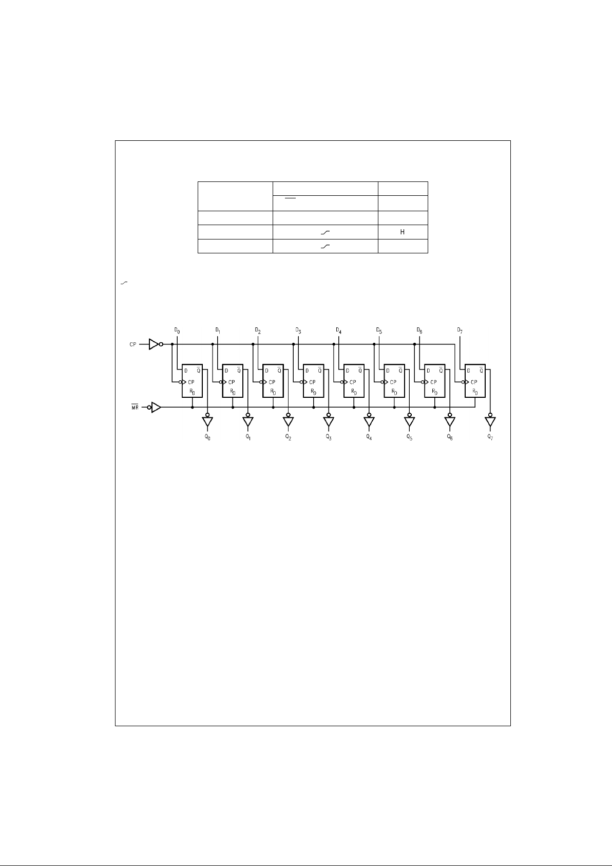
Logic Diagram
Please note that this diagram is provided only f or t he understanding of logic operations and should no t be us ed to estimate propagation delays.
Operating Mode Inputs Outputs
MR
CP D
n
Q
n
Reset (Clear) L X X L
Load ’1’ H
HH
Load ’0’ H
LL
 Loading...