Fairchild Semiconductor 74LVX174SJX, 74LVX174SJ, 74LVX174MX, 74LVX174MTCX, 74LVX174MTC Datasheet
...
May 1993
Revised March 1999
74LVX174 Low Voltage Hex D-Type Flip-Flop with Master Reset
© 1999 Fairchild Semiconductor Corporation DS011607.prf www.fairchildsemi.com
74LVX174
Low Voltage Hex D-Type Flip-Flop with Master Reset
General Description
The LVX174 is a high-speed hex D fli p-flop. The de vice is
used primarily as a 6-b it edge-triggered storage register.
The information on the D inputs is transferre d to storage
during the LOW-to-HIGH clock transition. The device has a
Master Reset to simultaneously clear all flip-flops.
Features
■ Input voltage level translation from 5V to 3V
■ Ideal for low power/low noise 3.3V applications
■ Guaranteed simultaneous switching noise level and
dynamic threshold performance
Ordering Code:
Devices also availab le in Tape and Reel. Specify by appending th e s uffix let t er “X” to the ordering code.
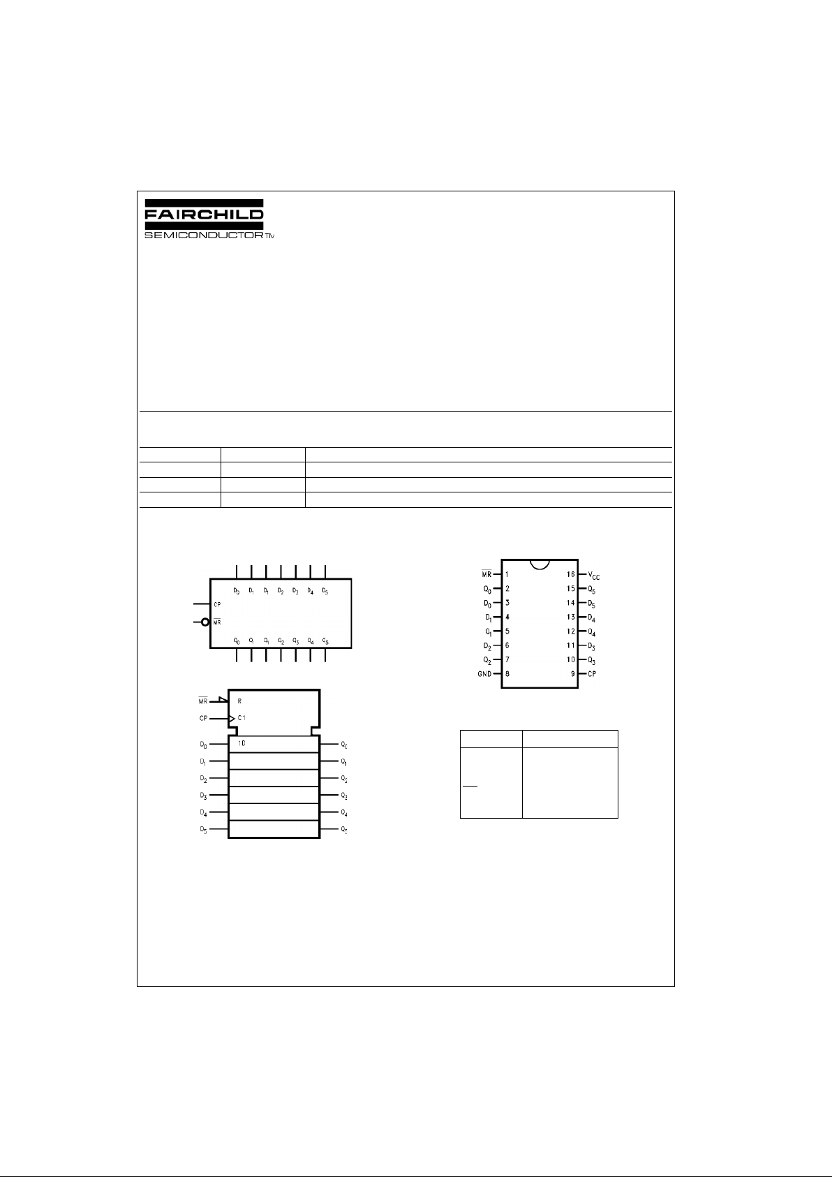
Logic Symbols
IEEE/IEC
Connection Diagram
Pin Descriptions
Order Number Package Number Package Description
74LVX174M M16A 16-Lead Small Outline Integrated Circuit (SOIC), JEDEC MS-012, 0.150” Narrow
74LVX174SJ M16D 16-Lead Small Outline Package (SOP), EIAJ TYPE II, 5.3mm Wide
74LVX174MTC MTC16 16-Lead Thin Shrink Small Outline Package (TSSOP), JEDEC MO-153, 4.4mm Wide
Pin Names Description
D
0–D5
Data Inputs
CP Clock Pulse Input
MR
Master Reset Input
Q
0–Q5
Outputs

www.fairchildsemi.com 2
74LVX174
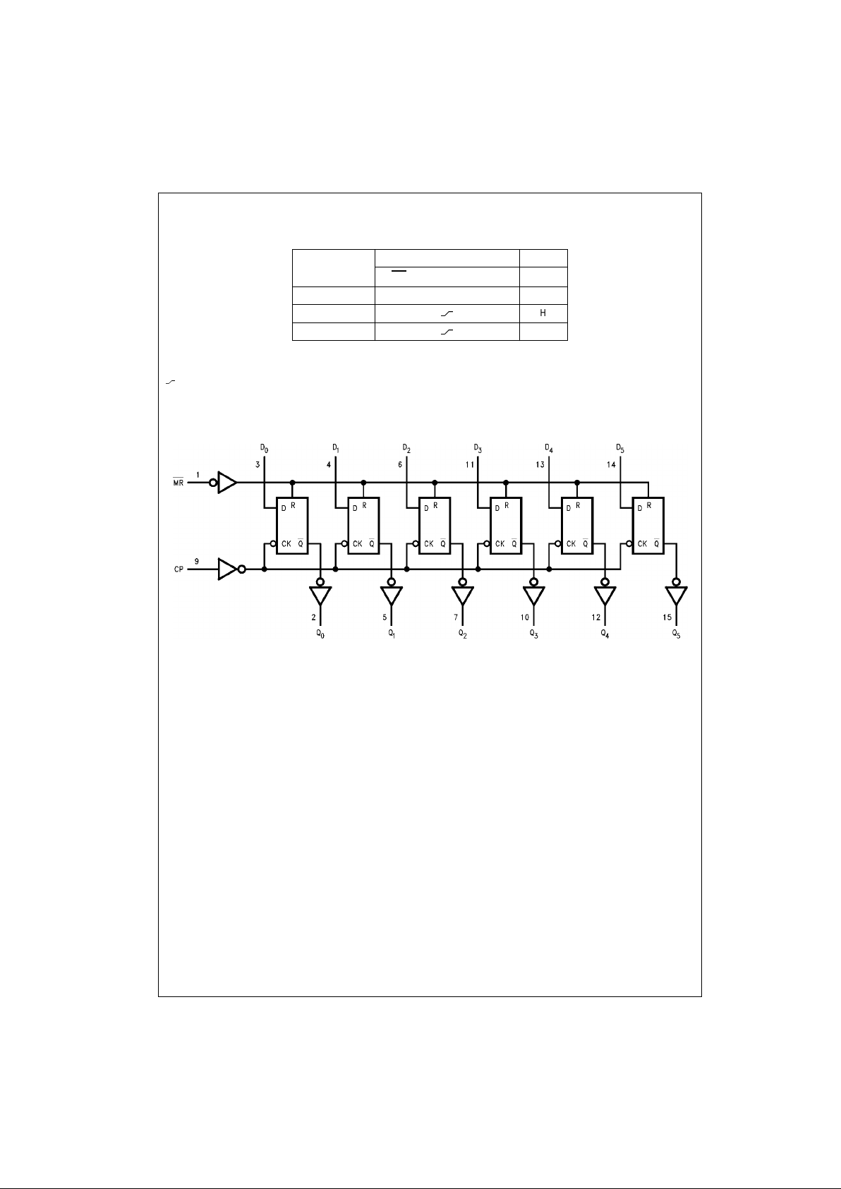
Truth Table
H = HIGH Voltage Level
L = LOW Voltage Level
X = Immaterial
= LOW-to-HIGH Transitio n
Logic Diagram
Operating Mode
Inputs Outputs
MR
CP
D
n
Q
n
Reset (Clear) L X X L
Load ‘1’ H
HH
Load ‘0’ H
LL
 Loading...