Fairchild Semiconductor 74LVX14MTC, 74LVX14MSCX, 74LVX14M, 74LVX14SJX, 74LVX14SJ Datasheet
...
© 1999 Fairchild Semiconductor Corporation DS011603 www.fairchildsemi.com
March 1993
Revised December 1999
74LVX14 Low Voltage Hex Inverter with Schmitt Trigger Input
74LVX14
Low Voltage Hex Inverter with Schmitt Trigger Input
General Description
The LVX14 contains six inverter gates each with a Schmitt
trigger input. They are capable of transforming slowly
changing input signals in to sharply defined, jitte r-free output signals. In additio n, they have a greater no ise margin
than conventional inverters.
The LVX14 has hysteresis between the positi ve-going a nd
negative-going input thresholds (typically 1.0V) which is
determined internall y by transistor ratios an d is essentially
insensitive to temperature and supply voltage variations.
The inputs tolerate voltages up to 7V allowing the interface
of 5V systems to 3V systems.
Features
■ Input voltage level translation from 5V to 3V
■ Ideal for low power/low noise 3.3V applications
■ Guaranteed simultaneous switching noise level and
dynamic threshold performance
Ordering Code:
Devices also availab le in Tape and Reel. Specify by appending su ffix let te r “X” to the ordering code .
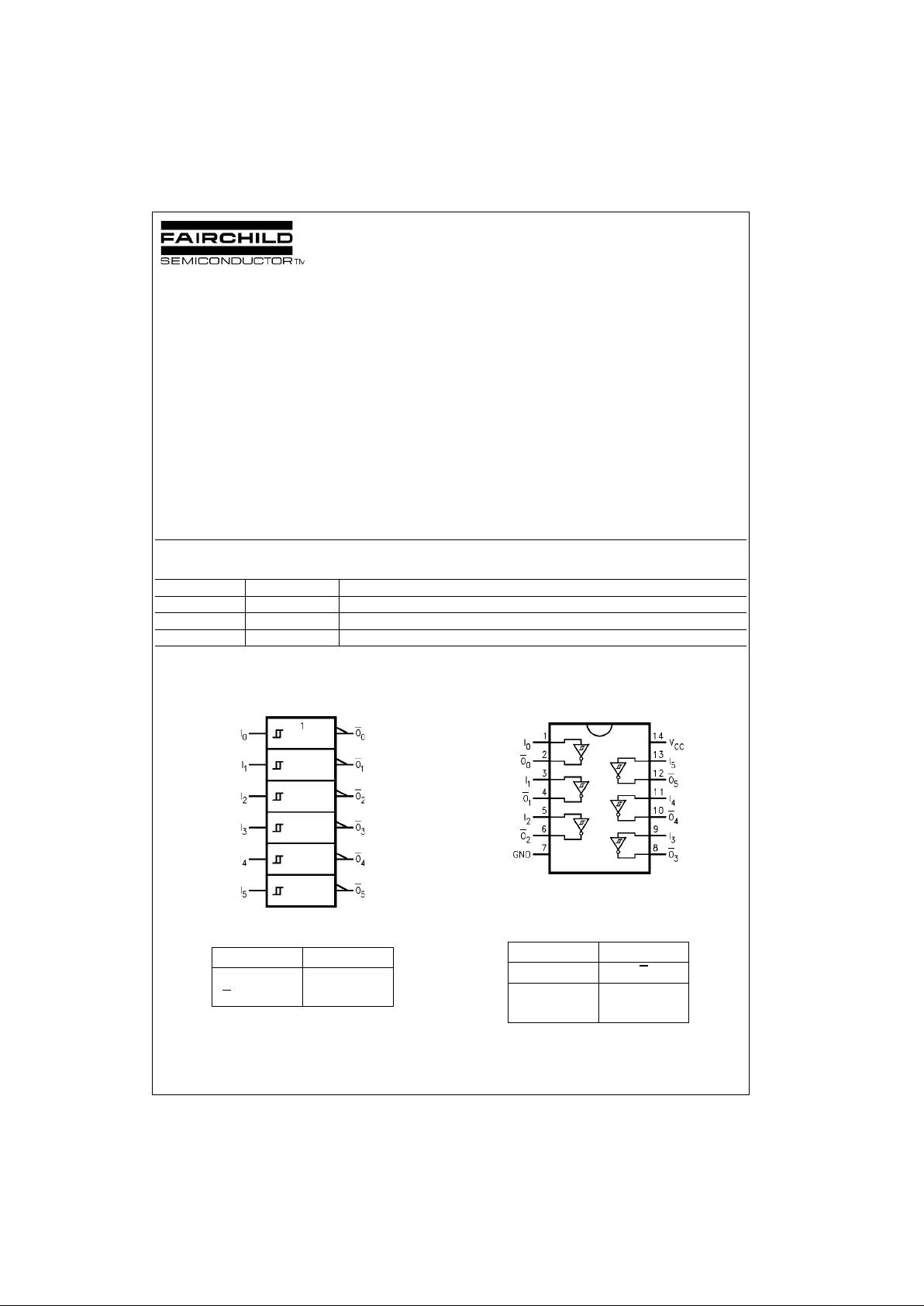
Logic Symbol
IEEE/IEC
Pin Descriptions
Connection Diagram
Truth Table
Order Number Package Number Package Description
74LVX14M M14A 14-Lead Small Outline Integrated Circuit (SOIC), JEDEC MS-120, 0.150” Narrow
74LVX14SJ M14D 14-Lead Small Outline Package (SOP), EIAJ TYPE II, 5.3mm Wide
74LVX14MTC MTC14 14-Lead Thin Shrink Small Outline Package (TSSOP), JEDEC MO-153, 4.4mm Wide
Pin Names Description
I
n
Inputs
O
n
Outputs
Input Output
AO
LH
HL

www.fairchildsemi.com 2
74LVX14
Absolute Maximum Ratings(Note 1) Recommended Operating
Conditions
(Note 2)
Note 1: The “Absolute Maximum Ratin gs” are those v alues beyon d which
the safety of the dev ice cannot be guaranteed. T he device sh ould not be
operated at these limits. The parametric values defined in the Electrical
Characteristics tables are not guaranteed at the absolute maximum ratings.
The “Recommend ed O peratin g Cond itions” t able w ill defin e the co ndition s
for actual device operation.
Note 2: Unused inputs must be held HIGH or LOW. They may not float.
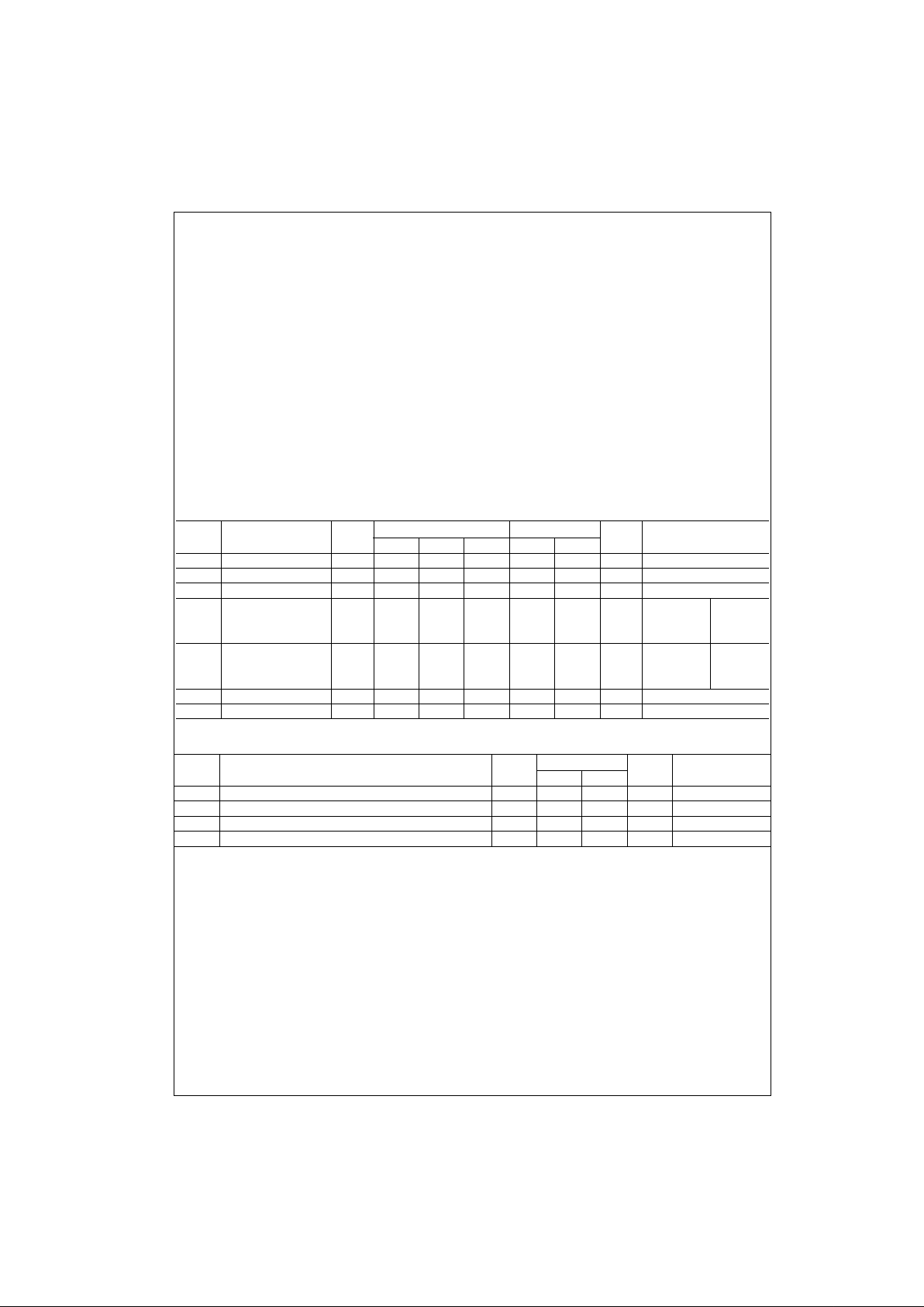
DC Electrical Characteristics
Noise Characteristics
(Note 3)
Note 3: Input tr = tf = 3ns
Supply Voltage (VCC) −0.5V to +7.0V
DC Input Diode Current (I
IK
)
V
I
= −0.5V −20 mA
DC Input Voltage (V
I
) −0.5V to 7V
DC Output Diode Current (I
OK
)
V
O
= −0.5V −20 mA
V
O
= VCC + 0.5V +20 mA
DC Output Voltage (V
O
) −0.5V to VCC + 0.5V
DC Output Source
or Sink Current (I
O
) ±25 mA
DC V
CC
or Ground Current
(I
CC
or I
GND
) ±50 mA
Storage Temperature (T
STG
) −65°C to +150°C
Power Dissipation 180 mW
Supply Voltage (V
CC
) 2.0V to 3.6V
Input Voltage (V
I
)0V to 5.5V
Output Voltage (V
O
) 0V to V
CC
Operating Temperature (TA) −40°C to +85°C
Symbol Parameter
V
CC
TA = +25°CT
A
= −40°C to +85°C
Units Conditions
Min Typ Max Min Max
Vt+ Positive Threshold 3.0 2.2 2.2 V
Vt− Negative Threshold 3.0 0.9 0.9 V
V
H
Hysteresis 3.0 0.3 1.2 0.3 1.2 V
V
OH
HIGH Level 2.0 1.9 2.0 1.9 IOH = −50 µA
Output Voltage 3.0 2.9 3.0 2.9 V VIN = VIL or VIHIOH = −50 µA
3.0 2.58 2.48 IOH = −4 mA
V
OL
LOW Level 2.0 0.0 0.1 0.1 IOL = 50 µA
Output Voltage 3.0 0.0 0.1 0.1 V VIN = VIL or VIHIOL = 50 µA
3.0 0.36 0.44 IOL = 4 mA
I
IN
Input Leakage Current 3.6 ±0.1 ±1.0 µAVIN = 5.5V or GND
I
CC
Quiescent Supply Current 3.6 2.0 20 µAVIN = VCC or GND
Symbol Parameter
V
CC
(V)
TA = 25°C
Units
CL (pF)
Typ Limit
V
OLP
Quiet Output Maximum Dynamic V
OL
3.3 0.3 0.5 V 50
V
OLV
Quiet Output Minimum Dynamic V
OL
3.3 −0.3 −0.5 V 50
V
IHD
Minimum HIGH Level Dynamic Input Voltage 3.3 2.0 V 50
V
ILD
Maximum LOW Level Dynamic Input Voltage 3.3 0.8 V 50
 Loading...