Fairchild Semiconductor 74LVX138SJX, 74LVX138SJ, 74LVX138MX, 74LVX138MTCX, 74LVX138MTC Datasheet
...
June 1993
Revised March 1999
74LVX138 Low Voltage 1-of-8 Decoder/Demultiplexer
© 1999 Fairchild Semiconductor Corporation DS011615.prf www.fairchildsemi.com
74LVX138
Low Voltage 1-of-8 Decoder/Demultiplexer
General Description
The LVX138 is a high-sp eed 1 -of-8 deco der/de mul tiplex er.
This device is ideally suited for high-speed bipolar memory
chip select address decoding. The multiple input enables
allow parallel expansion to a 1-of-24 decoder using just
three LVX138 devices or a 1-of-32 decoder using four
LVX138 devices and one inverter.
Features
■ Input voltage level translation from 5V to 3V
■ Ideal for low power/low noise 3.3V applications
■ Guaranteed simultaneous switching noise level and
dynamic threshold performance
Ordering Code:
Devices also availab le in Tape and Reel. Specify by appending su ffix let te r “X” to the ordering code.
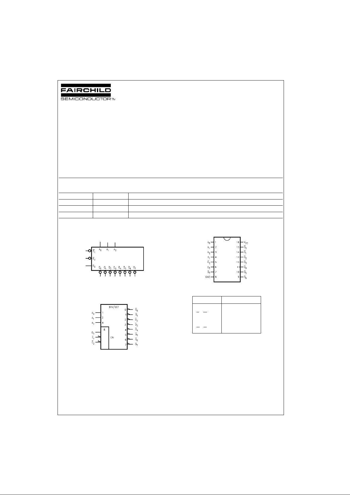
Logic Symbols
IEEE/IEC
Connection Diagram
Pin Descriptions
Order Number Package Number Package Description
74LVX138M M16A 16-Lead Small Outline Integrated Circuit (SOIC), JEDEC MS-012, 0.150” Narrow
74LVX138SJ M16D 16-Lead Small Outline Package (SOP), EIAJ TYPE II, 5.3mm Wide
74LVX138MTC MTC16 16-Lead Thin Shrink Small Outline Package (TSSOP), JEDEC MO-153, 4.4mm Wide
Pin Names Description
A
0–A2
Address Inputs
E
1
– E
2
Enable Inputs
E
3
Enable Input
O
0–O7
Outputs

www.fairchildsemi.com 2
74LVX138
Functional Description
The LVX138 high-speed 1-of-8 decoder/demultiplexer
accepts three binary weighted inputs (A
0
, A1, A2) and,
when enabled, provides eight mutually exclusive activeLOW outputs (O
0–O7
). The LVX138 features three Enable
inputs, two active-LOW (E
1
, E2) and one active-HIGH (E3).
All outputs will be HIGH unless E
1
and E2 are LOW and E
3
is HIGH.
The LVX138 can be used as an 8-out put demultip lexer by
using one of the a ctive LOW Enable inputs as the data
input and the othe r Enable input s as strobes. The Enable
inputs which are not used must be permanently tied to their
appropriate active-HIGH or active-LOW state.
Truth Table
H = HIGH Voltage Level
L = LOW Voltage Level
X = Immaterial
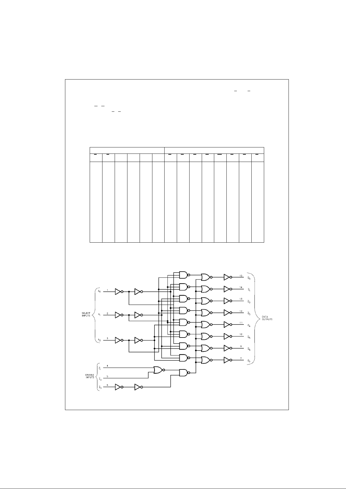
Logic Diagram
Please note that this diagram is provided only f or t he understanding of logic operations and should not be used to estimate propagation delays.
Inputs Outputs
E
1E2 E3A0A1 A2O0O1O2O3 O4O5O6O7
HXXXXXHHHHHHHH
XHXXXXHHHHHHHH
XXLXXXHHHHHHHH
LLHL LL LHHHHHHH
LLHHLLHLHHHHHH
LLHLHLHHLHHHHH
LL HHHL HHHLHHHH
LLHL LHHHHHLHHH
LLHHLHHHHHHLHH
LLHLHHHHHHHHLH
LLHHHHHHHHHHHL
 Loading...