Fairchild Semiconductor 74LVX132SJX, 74LVX132SJ, 74LVX132MX, 74LVX132MTCX, 74LVX132MTC Datasheet
...
October 1996
Revised March 1999
74LVX132 Low Voltage Quad 2-Input NAND Schmitt Trigger
© 1999 Fairchild Semiconductor Corporation DS012159.prf www.fairchildsemi.com
74LVX132
Low Voltage Quad 2-Input NAND Schmitt Trigger
General Description
The LVX132 contains four 2-input NAND Schmitt Trigger
Gates. The pin configu ration a nd fun ction are the sa me as
the LVX00 but the inputs have hysteresis between the positive-going and negat ive-going input thresholds, which are
capable of transforming slowl y changing input signa ls into
sharply defined, jitter-free output signals, thus providing
greater noise margins than conventional gates.
The inputs tolerate voltages up to 7V allowing the interface
of 5V systems to 3V systems.
Features
■ Input voltage level translation from 5V to 3V
■ Ideal for low power/low noise 3.3V applications
■ Guaranteed simultaneous switching noise level and
dynamic threshold performance
Ordering Code:
Devices also availab le in Tape and Reel. Specify by appending su ffix let te r “X” to the ordering code.
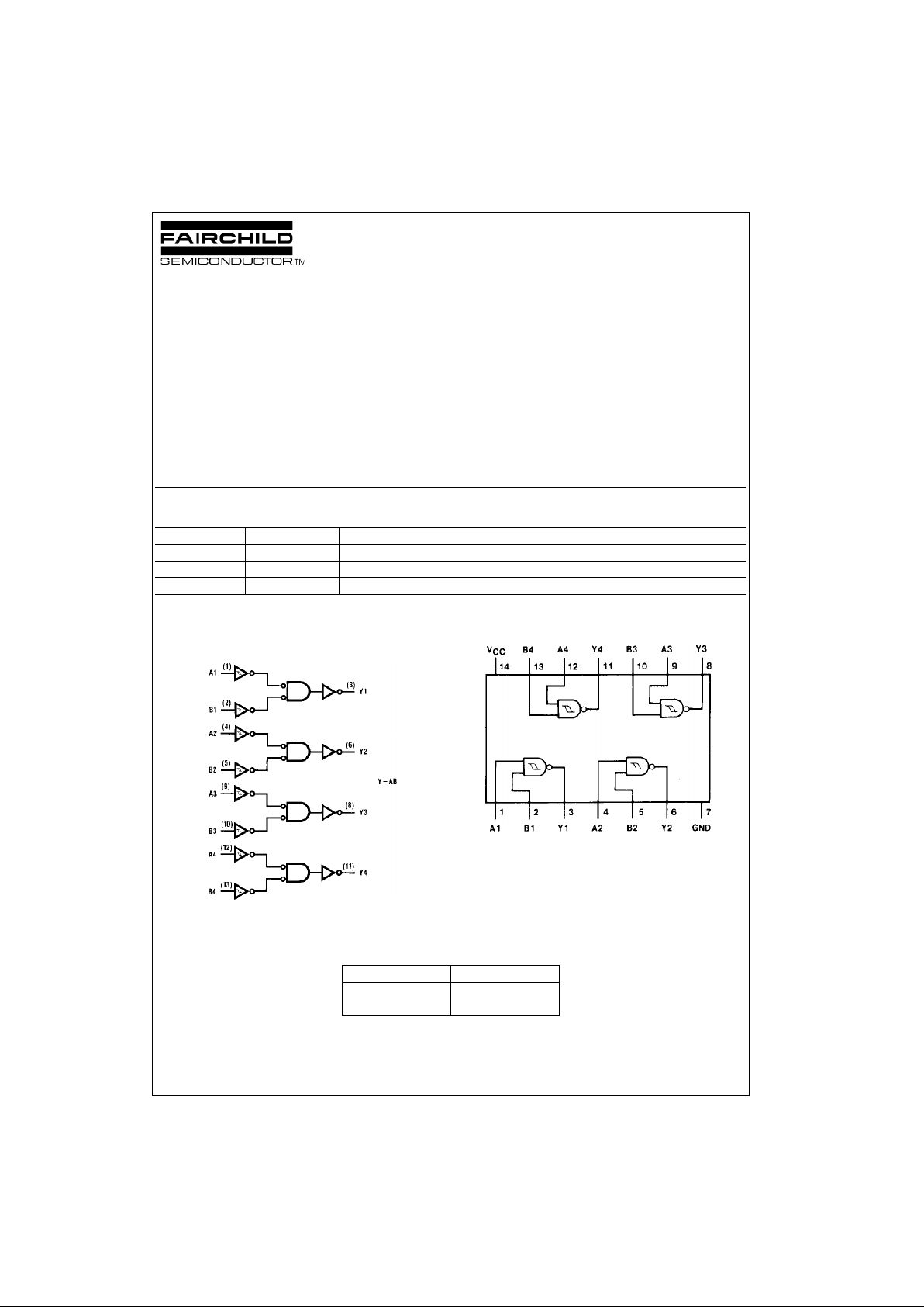
Logic Diagram Connection Diagram
Pin Descriptions
Order Number Package Number Package Description
74LVX132M M14A 14-Lead Small Outline Integrated Circuit (SOIC), JEDEC MS-120, 0.150” Narrow
74LVX132SJ M14D 14-Lead Small Outline Package (SOP), EIAJ TYPE II, 5.3mm Wide
74LVX132MTC MTC14 14-Lead Thin Shrink Small Outline Package (TSSOP), JEDEC MO-153, 4.4mm Wide
Pin Names Descriptions
A
n
, B
n
Inputs
Y
n
Outputs

www.fairchildsemi.com 2
74LVX132
Absolute Maximum Ratings(Note 1) Recommended Operating
Conditions
(Note 2)
Note 1: The “Absolute Maximum Ratin gs” are those v alues beyon d which
the safety of the dev ice cannot be guaranteed. T he device sh ould not be
operated at these limits. The parametric values defined in the Electrical
Characteristics tables are not guaranteed at the absolute maximum ratings.
The “Recommend ed O peratin g Cond itions” t able w ill defin e the co ndition s
for actual device operation.
Note 2: Unused inputs must be held HIGH or LOW. They may not float.
DC Electrical Characteristics
Noise Characteristics
(Note 3)
Note 3: Input tr = tf = 3 ns
Supply Voltage (VCC) −0.5V to +7.0V
DC Input Diode Current (I
IK
)
V
I
= −0.5V −20 mA
DC Input Voltage (V
I
) −0.5V to 7V
DC Output Diode Current (I
OK
)
V
O
= −0.5V −20 mA
V
O
= VCC + 0.5V +20 mA
DC Output Voltage (V
O
) −0.5V to VCC + 0.5V
DC Output Source
or Sink Current (I
O
) ±25 mA
DC V
CC
or Ground Current
(I
CC
or I
GND
) ±50 mA
Storage Temperature (T
STG
) −65°C to +150°C
Power Dissipation 180 mW
Supply Voltage (V
CC
) 2.0V to 3.6V
Input Voltage (V
I
) 0V to 5.5V
Output Voltage (V
O
) 0V to V
CC
Operating Temperature (TA) −40°C to +85°C
Input Rise and Fall Time (∆t/∆V) 0 ns/V to 100 ns/V
Symbol Parameter
V
CC
TA = +25°CT
A
= −40°C to +85°C
Units Conditions
Min Typ Max Min Max
Vt+ Positive Threshold 3.0 2.2 2.2 V
Vt− Negative Threshold 3.0 0.9 0.9 V
V
H
Hysteresis 3.0 0.3 1.2 0.3 1.2 V
V
OH
HIGH Level 2.0 1.9 2.0 1.9 VIN = VIL or VIHIOH = −50 µA
Output Voltage 3.0 2.9 3.0 2.9 V IOH = −50 µA
3.0 2.58 2.48 IOH = −4 mA
V
OL
LOW Level 2.0 0.0 0.1 0.1 VIN = VIL or VIHIOL = 50 µA
Output Voltage 3.0 0.0 0.1 0.1 V IOL = 50 µA
3.0 0.36 0.44 IOL = 4 mA
I
IN
Input Leakage Current 3.6 ±0.1 ±1.0 µAVIN = 5.5V or GND
I
CC
Quiescent Supply Current 3.6 2.0 20 µAVIN = VCC or GND
Symbol Parameter
V
CC
(V)
TA = 25°C
Units
CL (pF)
Typ Limit
V
OLP
Quiet Output Maximum Dynamic V
OL
3.3 0.3 0.5 V 50
V
OLV
Quiet Output Minimum Dynamic V
OL
3.3 −0.3 −0.5 V 50
V
IHD
Minimum HIGH Level Dynamic Input Voltage 3.3 2.0 V 50
V
ILD
Maximum LOW Level Dynamic Input Voltage 3.3 0.8 V 50
 Loading...