Fairchild Semiconductor 74LVTH16245MTDX, 74LVTH16245MTD, 74LVTH16245MEAX, 74LVTH16245MEA, 74LVT16245MTDX Datasheet
...
January 1999
Revised November 1999
74LVT16245 • 74LVTH16245
Low Voltage 16-Bit Transceiver with 3- STATE Outputs
74LVT16245 • 74LVTH16245 Low Voltage 16-Bit Tr ansceiver with 3-STA TE Outputs
General Description
The LVT16245 and LVTH16245 contain sixteen non-inverting bidirectional buffers with 3-STATE outputs and is
intended for bus orien ted applications. The de vice is byte
controlled. Each byte has separate control inputs which
can be shorted toget her for full 16-bit ope ration. The T/R
inputs determine the direction of data flow through the
device. The OE
placing them in a high impedance state.
The LVTH16245 data inputs includ e bushold, eliminating
the need for external pull-up resistors to hold unused
inputs.
These non-inverting transceivers are designed for low-voltage (3.3V) V
vide a TTL interface to a 5V environment. Th e LVT16245
and LVTH16245 are fabricated with an adva nced B iCMOS
technology to achieve high speed ope ration similar to 5V
ABT while maintaining low power dissipation.
inputs disable bo th the A and B ports by
applications, but with the capability to pro-
CC
Features
■ Input and output interface capability to systems at
5V V
CC
■ Bushold data inputs elimi nate th e need fo r extern al pullup resistors to hold unused inputs (74LVTH16245), also
available without bushold feat ure (74LVT16245).
■ Live insertion/extraction per mi tt ed
■ Power Up/Down high impedance provides glitch-free
bus loading
■ Outputs source/sink −32 mA/+64 mA
■ Functionally compatible with the 74 series 16245
■ Latch-up performance exce eds 500 mA
Ordering Code:
Order Number
74LVT16245MEA MS48A 48-Lead Small Shrink Outline Package (SSOP), JEDEC MO-118, 0.300” Wide
74LVT16245MTD MTD48 48-Lead Thin Shrink Small Outline Package (TSSOP), JEDEC MO-153, 6.1mm Wide
74LVTH16245MEA MS48A 48-Lead Small Shrink Outline Package (SSOP), JEDEC MO-118, 0.300” Wide
74LVTH16245MTD MTD48 48-Lead Thin Shrink Small Outline Package (TSSOP), JEDEC MO-153, 6.1mm Wide
Devices also availab l e in Tape and Reel. Specify by appending su ffix let te r “X” to the ordering code.
Package
Number
Package Descript ion
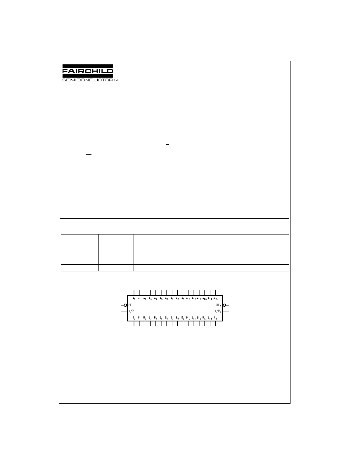
Logic Symbol
© 1999 Fairchild Semiconductor Corporation DS500152 www.fairchildsemi.com

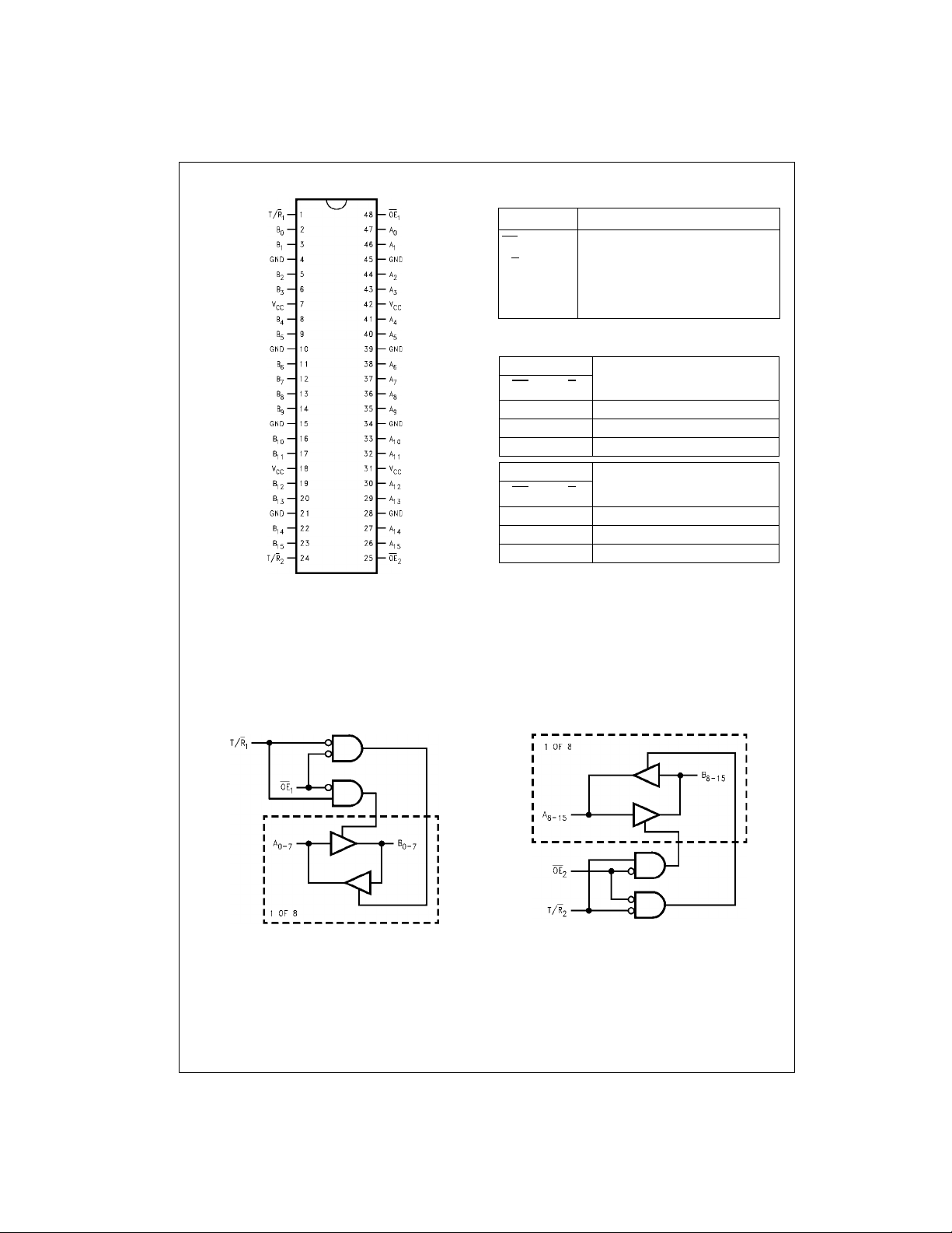
Connection Diagram Pin Descriptions
Pin Names Description
OE
T/R
A
0–A15
B
0–B15
n
n
Output Enable Input (Active LOW)
Transmit/Receive Input
Side A Inputs/3-STATE Outputs
Side B Inputs/3-STATE Outputs
Truth Tables
74LVT16245 • 74LVTH16245
Inputs
OE
T/R
1
1
L L Bus B0–B7 Data to Bus A0–A
L H Bus A0–A7 Data to Bus B0–B
H X HIGH–Z State on A0–A7,B0–B
Inputs
OE
T/R
2
2
L L Bus B8–B15 Data to Bus A8–A
L H Bus A8–A15 Data to Bus B8–B
HXHIGH–Z State on A8–A15,B8–B
H = HIGH Voltage Level
L = LOW Voltage Level
X = Immaterial
Z = High Impedance
Outputs
Outputs
Functional Description
The LVT16245 and LVTH16245 contain sixteen non-inverting bidirectional buffers with 3-STA T E outputs. The device is byte
controlled with eac h byte functioning identically, but independent of the other. The control pins can be sho rted together to
obtain full 16-bit operation.
7
7
7
15
15
15
Logic Diagrams
Note: Please note that these diagrams are provided only for the understanding of logic operations and should not be used to estimat e propagation delays.
www.fairchildsemi.com 2
 Loading...