Fairchild Semiconductor 74LVTH16244MTD, 74LVTH16244MEAX, 74LVTH16244MEA, 74LVTH16244MTDX Datasheet

© 1999 Fairchild Semiconductor Corporation DS500151 www.fairchildsemi.com
Print form created on April 12, 1999 2:43 pm
March 1999
Revised April 1999
74LVT16244 • 74LVTH16244 Low Voltage16-Bit Buffer/Line Driver with 3-STATE Outputs
74LVT16244 • 74LVTH16244
Low Voltage16-Bit Buffer/Line Driver
with 3-STATE Outputs
General Description
The LVT16244 and LVTH16244 contain sixteen non-inverting buffers with 3-STATE outputs designed to be employed
as a memory and address driver, clock driver, or bus oriented transmitter/rece iver. The device is nibble controlled.
Individual 3-STATE control inputs can be shorte d together
for 8-bit or 16-bit operation.
The LVTH16244 data inputs includ e bushold, eliminating
the need for external pull-up resistors to hold unused
inputs.
These buffers and line drivers are designed for low-voltage
(3.3V) V
CC
applications, but with the capability to provide a
TTL interface to a 5V environment. The LVT16244 and
LVTH16244 are fabricated with an advanced BiCMOS
technology to achieve high speed operation si milar to 5V
ABT while maintaining a low power dissipation
Features
■ Input and output interface capa bility to systems at 5V
V
CC
■ Bushold data inputs elimina te the nee d for exte rnal pul lup resistors to hold unused inputs (74LVTH16244), also
available without bushold feature (74LVT16244).
■ Live insertion/extraction per mitt ed
■ Power Up/Down high impedance provides glitch-free
bus loading
■ Outputs source/sink −32 mA/+64 mA
■ Functionally compatible with the 74 series 16244
■ Latch-up performance exceeds 500 mA
Ordering Code:
Device also available in Tape and Reel. Specify by appending su ffix le tter “X” to the ordering code.
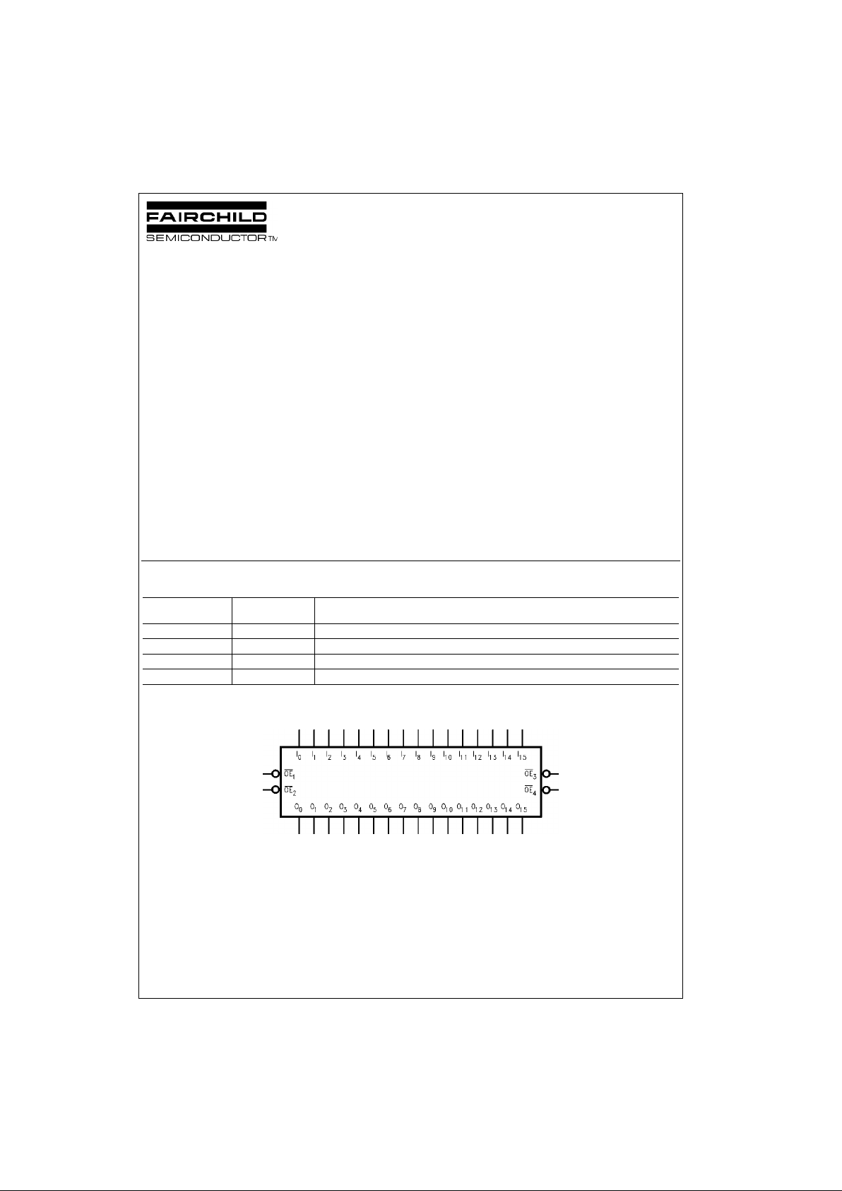
Logic Symbol
Order Number Package
Number
Package Descript ion
74LVT16244MEA MS48A 48-Lead Small Shrink Outline Package (SSOP), JEDEC MO-118, 0.300” Wide
74LVT16244MTD MTD48 48-Lead Thin Shrink Small Outline Package (TSSOP), JEDEC MO-153, 6.1mm Wide
74LVTH16244MEA MS48A 48-Lead Small Shrink Outline Package (SSOP), JEDEC MO-118, 0.300” Wide
74LVTH16244MTD MTD48 48-Lead Thin Shrink Small Outline Package (TSSOP), JEDEC MO-153, 6.1mm Wide

www.fairchildsemi.com 2
74LVT16244 • 74LVTH16244
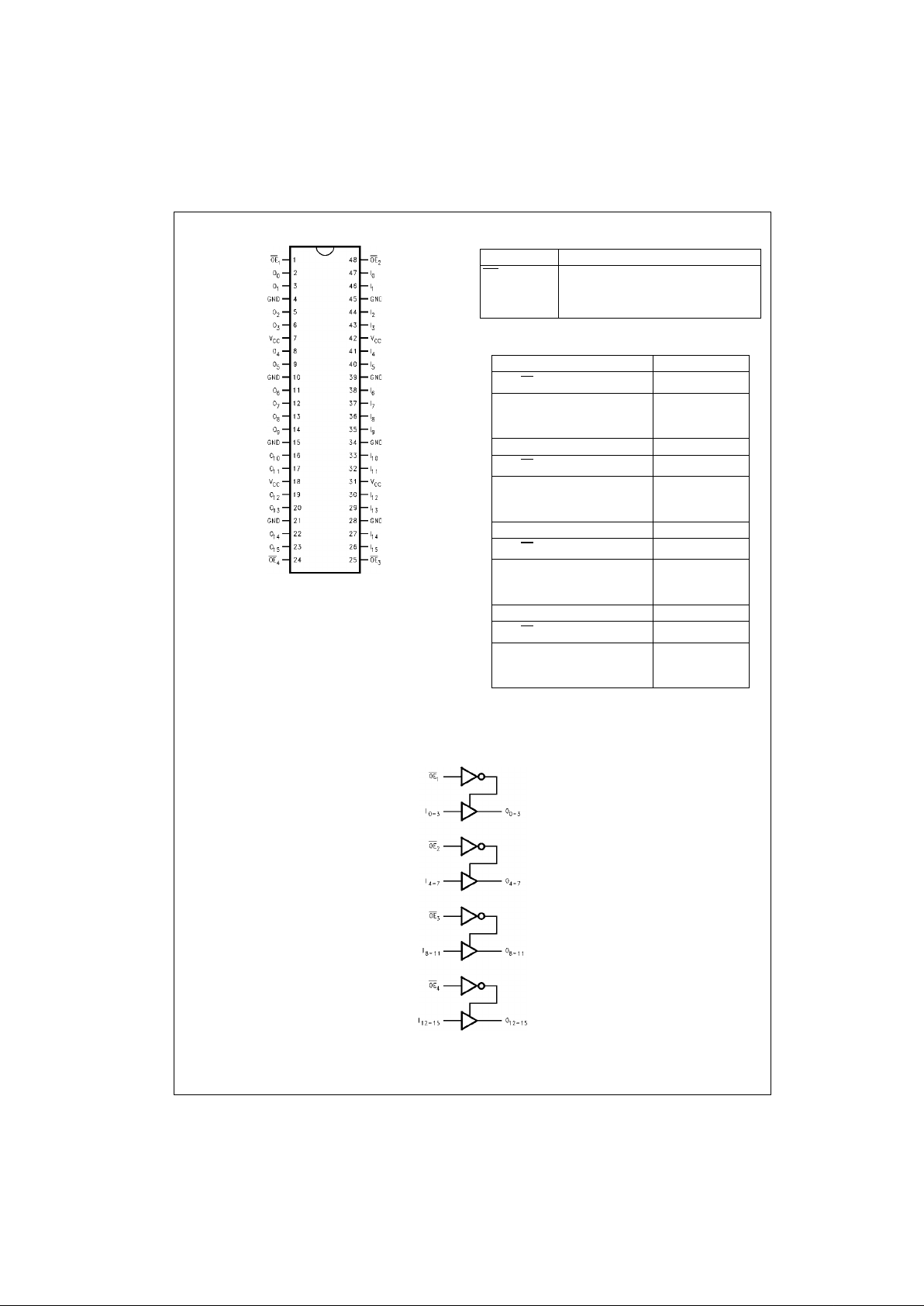
Connection Diagram
Functional Description
The LVT16244 and LVTH16244 contain sixteen non-inverting buffers with 3 -STATE outputs. The devi ce is nibble (4
bits) controlled with ea ch nibble functi oning identically, but
independent of the oth er. The control pins can be shorted
together to obtain full 16-bit operation.
Pin Descriptions
Tr uth Table
H = High Voltage Level
L = Low Voltage Level
X = Immaterial
Z = High Impedance
Logic Diagram
Pin Names Description
OE
n
Output Enable Inputs (Active Low)
I
0–I15
Inputs
O
0–O15
Outputs
Inputs Outputs
OE
1
I0–I
3
O0–O
3
LL L
LH H
HX Z
Inputs Outputs
OE
2
I4–I
7
O4–O
7
LL L
LH H
HX Z
Inputs Outputs
OE
3
I8–I
11
O8–O
11
LL L
LH H
HX Z
Inputs Outputs
OE
4
I12–I
15
O12–O
15
LL L
LH H
HX Z
 Loading...