Fairchild Semiconductor 74LVTH16240MTDX, 74LVTH16240MTD, 74LVTH16240MEAX, 74LVTH16240MEA, 74LVT16240MTDX Datasheet
...
March 1999
Revised March 1999
74LVT16240 • 74LVTH16240
Low Voltage 16-Bit Inverting Buffer/Line Driver
with 3-STATE Outputs
74LVT16240 • 74LVTH16240 Low Voltage 16-Bit Inverting Buffer/Line Driver with 3-STATE Outputs
General Description
The LVT16240 and LVTH16240 contain sixteen invert ing
buffers with 3-STATE outputs designed to be empl oyed as
a memory and address dr iver, clock driver, or bus-orient ed
transmitter/receiver. The device is nibble controlled.
Individual 3-STATE control inputs can be shorte d together
for 8-bit or 16-bit operation.
The LVTH16240 data inputs includ e bushold, eliminating
the need for external pull-up resistors to hold unused
inputs.
These buffers and line drivers are designed for low-voltage
(3.3V) V
TTL interface to a 5V environment. The LVT16240 and
LVTH16240 are fabricated with an advanced BiCMOS
applications, but with the capability to provide a
CC
technology to achieve high speed operation si milar to 5V
ABT while maintaining a low power dissipation.
Features
■ Input and output interface capability to systems at
5V V
CC
■ Bushold data inputs elimina te the nee d for exte rnal pullup resistors to hold unused inputs (74LVTH16240), also
available without bushold feature (74LVT16240).
■ Live insertion/extraction per mitt ed
■ Power Up/Down high impedance provides glitch-free
bus loading
■ Outputs source/sink −32 mA/+64 mA
■ Functionally compatible with the 74 series 16240
■ Latch-up performance exce eds 500 mA
Ordering Code:
Order Number
74LVT16240MEA MS48A 48-Lead Small Shrink Outline Package (SSOP), JEDEC MO-118, 0.300” Wide
74LVT16240MTD MTD48 48-Lead Thin Shrink Small Outline Package (TSSOP), JEDEC MO-153, 6.1mm Wide
74LVTH16240MEA MS48A 48-Lead Small Shrink Outline Package (SSOP), JEDEC MO-118, 0.300” Wide
74LVTH16240MTD MTD48 48-Lead Thin Shrink Small Outline Package (TSSOP), JEDEC MO-153, 6.1mm Wide
Devices also availab le in Tape and Reel. Specify by appending su ffix le tter “X” to the ordering code.
Package
Number
Package Descript ion
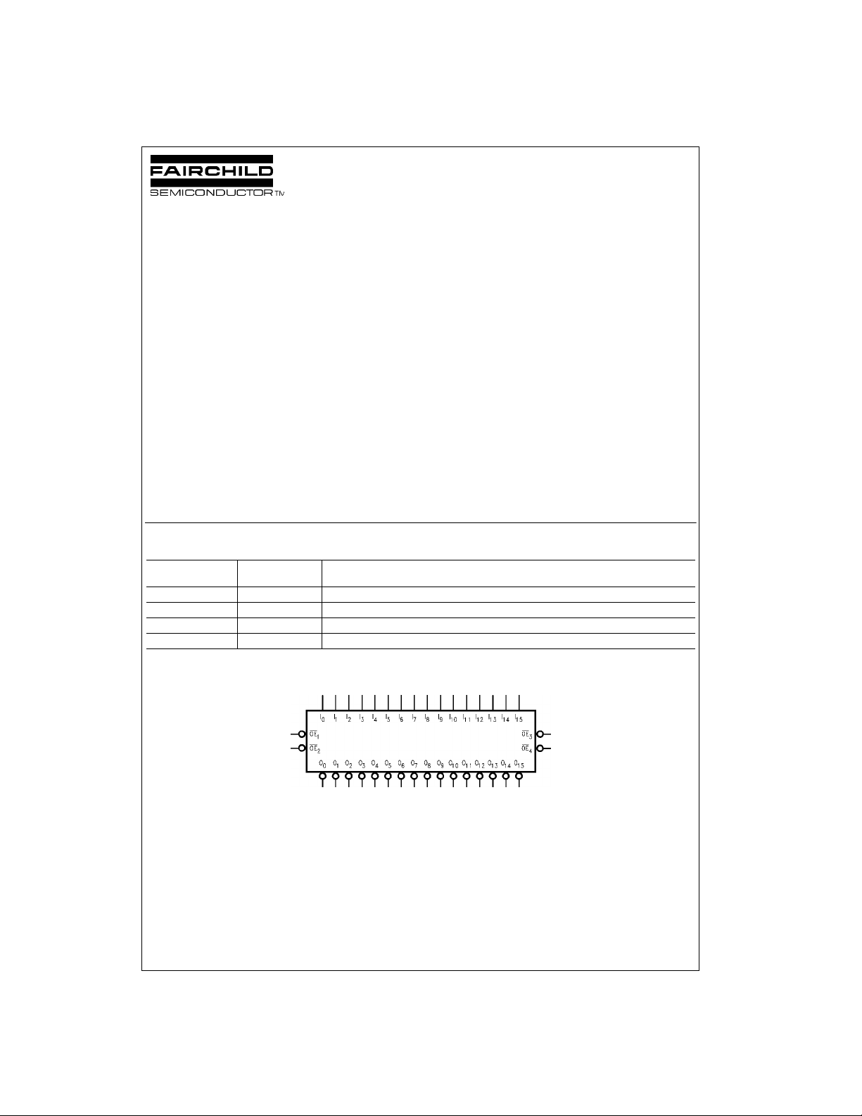
Logic Symbol
© 1999 Fairchild Semiconductor Corporation DS012025.prf www.fairchildsemi.com

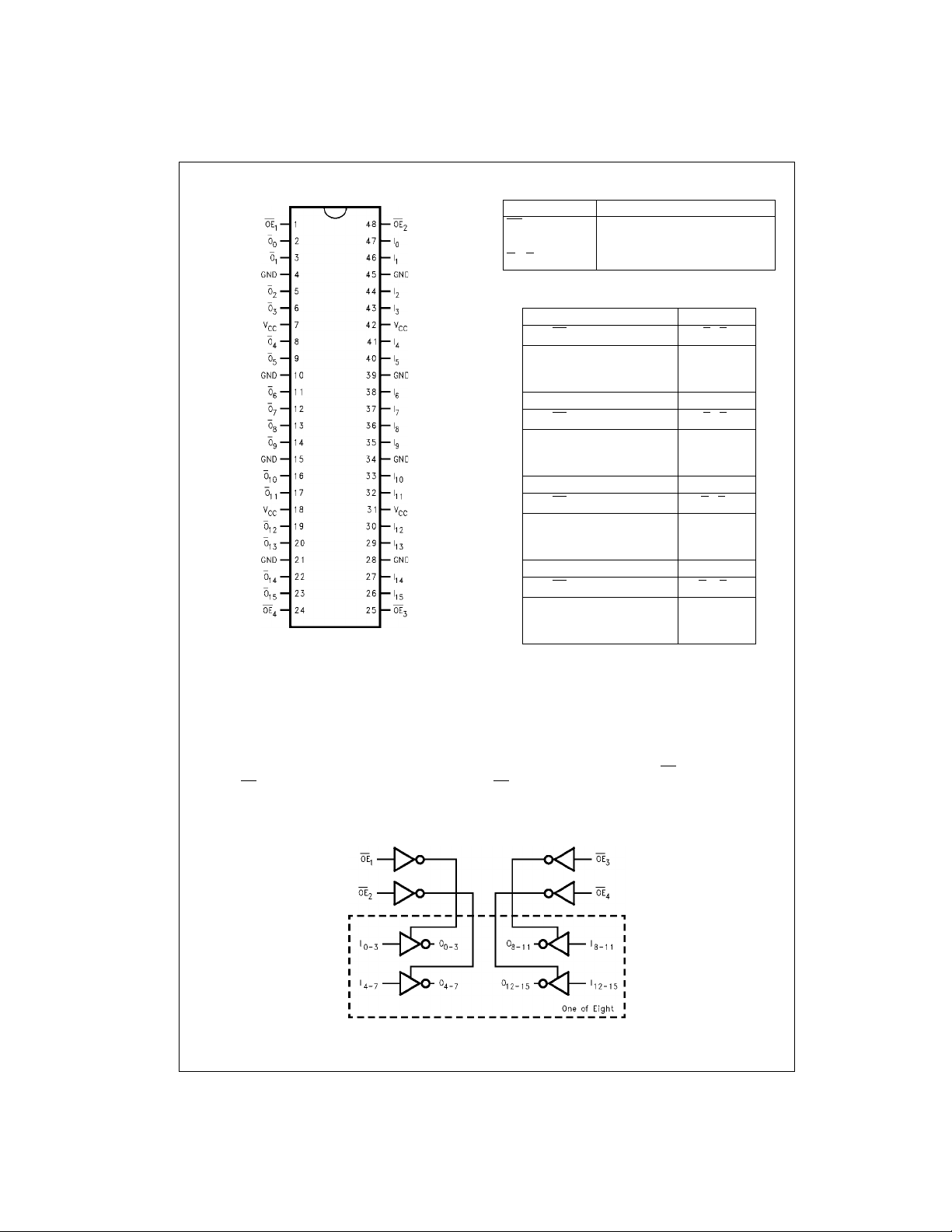
Connection Diagram Pin Descriptions
Pin Names Description
OE
n
I
0–I15
O
0–O15
Truth Table
OE
1
LLH
74LVT16240 • 74LVTH16240
H = High Voltage Level
L = Low Voltage Level
X = Immaterial
Z = High Impedance
LHL
HXZ
OE
2
LLH
LHL
HX Z
OE
3
LLH
LHL
HXZ
OE
4
LLH
LHL
HXZ
Output Enable Inputs (Active Low)
Inputs
3-STATE Outputs
Inputs Outputs
I0–I
3
O0–O
Inputs Outputs
I4–I
7
O4–O
Inputs Outputs
I8–I
11
O8–O
11
Inputs Outputs
I12–I
15
O12–O
3
7
15
Functional Description
The LVT16240 and LVTH16240 contain sixteen in verting bu ffers with 3-STATE standard outputs. The de vice is nibble (4
bits) controlled wit h each nibble functioning identica lly, but independent of the other. The control pins may be shorted
together to obtain f ull 16 -bit operat ion. The 3- STATE outputs are controlled by an Ou tput Enab le (O E
ble. When OE
is LOW, the outputs are in 2-state mode. When OEn is HIGH, the outputs are in the high impedance mode,
n
) input for each nib-
n
but this does not interfere with entering new data into the inputs.
Logic Diagram
Please note that this diagram is provided only for the understan ding of logic operation s and should not be used t o es t im ate propagation delays.
www.fairchildsemi.com 2
 Loading...