

Fairchild Semiconductor 74LVTH162374 Datasheet
74LVTH162374
Low Voltage 16-Bit D-Type Flip-Flop
with 3-STATE Outputs
and 25
Ω Series Resistors in the Outputs
June 2000
Revised August 2001
74LVTH162374 Low Voltage 16-Bit D-Type Fli p-Flop with 3-STATE Outputs and 25
Outputs
General Description
The LVTH162374 contains sixteen non-inverting D-type
flip-flops with 3-STATE outputs and is intended for bus oriented applications. The dev ice is byte controlled. A buffered clock (CP) and Output E nable (OE
each byte and can be shorted together for full 16-bit operation.
The LVTH162374 is designed with equival ent 25
resistance in both the HIGH and LOW states of th e o utp ut.
This design reduces line noise in applications such as
memory address drivers, clock d rivers, and bus transc eivers/transmitters.
The LVTH162374 data inputs includ e bushold, eliminat ing
the need for external pull-up resistors to hold unused
inputs.
These flip-flops are designed for low-voltage (3.3V) V
applications, but with the capability to provide a TTL inter-
face to a 5V enviro nment. The LVTH162374 is fabricated
with an advanced BiCMOS technology to achieve high
speed operation similar to 5V ABT while maintaining a low
power dissipation.
) are common to
Ω series
Features
■ Input and output interface capability to systems at
5V V
CC
■ Bushold data inputs eliminate the need for external
pull-up resistors to hold unused inputs
■ Live insertion/extraction per mi tt ed
■ Power Up/Power Down high impedance provides
glitch-free bus loading
■ Outputs include equiv alent series resistance of 25
make external termination resistors unnecessary and
reduce overshoot and undershoot
■ Functionally compatible with the 74 series 16374
■ Latch-up performance exce eds 500 mA
■ ESD performance:
CC
Human-body model
Machine model
Charged-device model
■ Also packaged in plastic Fine-Pitch Ball Grid Array
(FBGA) (Preliminary)
> 2000V
> 200V
> 1000V
Ω to
Ordering Code:
Order Number
74LVTH162374GX
(Note 1)
74LVTH162374MEA MS48A 48-Lead Small Shrink Outline Package (SSOP), JEDEC MO-118, 0.300" Wide
74LVTH162374MEX MS48A 48-Lead Small Shrink Outline Package (SSOP), JEDEC MO-118, 0.300" Wide
74LVTH162374MTD MTD48 48-Lead Thin Shrink Small Outline Package (TSSOP), JEDEC MO-153, 6.1mm Wide
74LVTH162374MTX MTD48 48-Lead Thin Shrink Small Outline Package (TSSOP), JEDEC MO-153, 6.1mm Wide
Note 1: BGA package available in Tape and Reel only.
Package
Number
BGA54A
(Preliminary)
Package Description
54-Ball Fine-Pitch Ball Grid Array (FBGA), JEDEC MO-205, 5.5mm Wide
[TAPE and REEL]
[TUBES]
[TAPE and REEL]
[TUBES]
[TAPE and REEL]
Ω
Series Resistors in the
© 2001 Fairchild Semiconductor Corporation DS500355 www.fairchildsemi.com
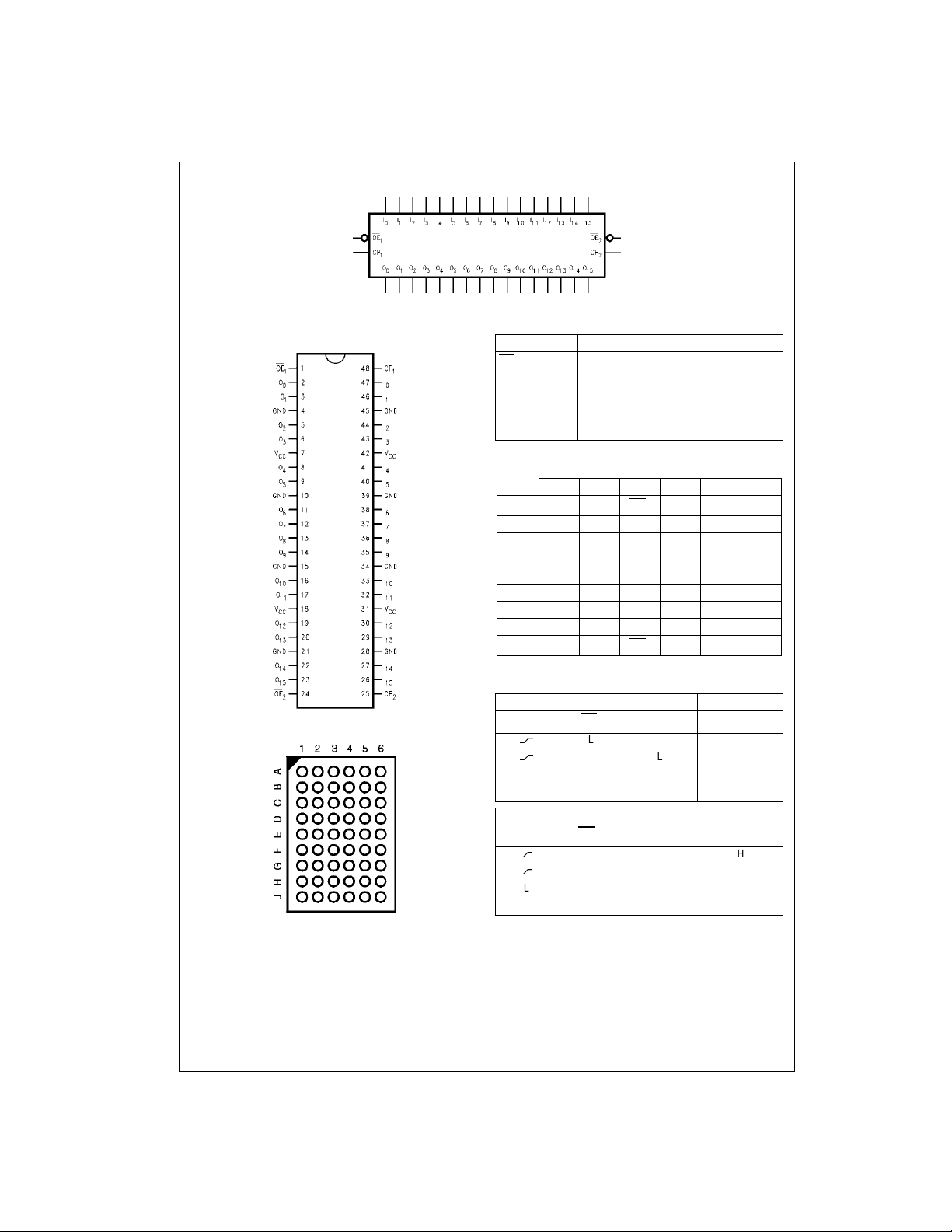
Logic Symbol
74LVTH162374
Connection Diagrams
Pin Assignments for SSOP and TSSOP
Pin Assignment for FBGA
(Top Thru View)
Pin Descriptions
Pin Names Description
OE
CP
I
0–I15
O
0–O15
n
n
Output Enable Input (Active LOW)
Clock Pulse Input
Inputs
3-STATE Outputs
NC No Connect
FBGA Pin Assignments
123456
A O
B O
C O
D O
E O
F O
G O
H O
J O
NC OE1CP1NC I
0
O1NC NC I
2
O3V
4
6
8
10
12O11VCCVCCI11
14O13
15
CCVCCI3
O5GND GND I
O7GND GND I
O9GND GND I
NC NC I
NC OE2CP2NC I
1
5
7
9
13I14
Truth Tables
Inputs Outputs
CP
1
LL X O
XH X Z
CP
2
LL X O
XH X Z
H = HIGH Voltage Level
L = LOW Voltage Level
X = Immaterial
Z = HIGH Impedance
Oo = Previous Oo before HIGH-to-LOW of CP
OE
1
I0–I
7
O0–O
LH H
LL L
Inputs Outputs
OE
2
I8–I
15
O8–O
LH H
LL L
0
I
2
I
4
I
6
I
8
I
10
I
12
15
7
o
15
o
www.fairchildsemi.com 2
Functional Description
The LVTH162374 consists of sixteen edge-trigger ed flip -flops with individ ual D-ty pe inp uts and 3-STATE true outputs. The
device is byte cont rolled with each byte functioning id entically, but independent of the other. The control pin s can be
shorted together to obtain f ull 16 -bit op erat ion. Each by te has a buffered clock and buffered Output Enab le comm on to a ll
flip-flops within that byte. The description which follows applies to each byte. Each flip-flop will store the state of their individual D-type inputs that m ee t th e s etup a nd ho ld tim e req uireme nts on the L OW-to-HIG H Clo ck ( CP
Output Enable (OE
the high impedance state. Operation of the OE
) LOW, the contents of the flip-flops are avail a ble at the ou tpu t s. When OEn is HIGH, the outputs go to
n
input does not affect the state of the flip-flops.
n
) transition. Wi th the
n
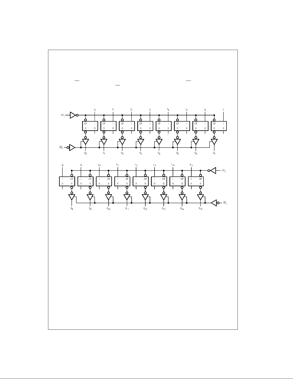
Logic Diagrams
Byte 1 (0:7)
Byte 2 (8:15)
74LVTH162374
Please note that these diagrams ar e provided for the understanding of logic operation and should not be used to estimate propagati on delays.
3 www.fairchildsemi.com
 Loading...