Fairchild Semiconductor 74LVTH162373 Datasheet

74LVTH162373
Low Voltage 16-Bit Transparent Latch with
3-STATE Outputs and
25
Ω Series Resistors in the Outputs
October 2000
Revised November 2000
74LVTH162373 Low Voltage 16-Bit Transparent Latch with 3-STATE Outputs and 25
Outputs
General Description
The LVTH162373 contains sixteen non-inverting latches
with 3-STATE outputs and is intended for bus oriented
applications. The device is byte controlled. The flip-flops
appear transparent to the data when the Latch Enable (LE)
is HIGH. When LE is LOW, the data that meets the setup
time is latched. Data appears o n the bus when th e Output
Enable (OE
a high impedance state.
The LVTH162373 is designed with equival ent 25
resistance in both the HIGH and LOW states of th e o utp ut.
This design reduces line noise in applications such as
memory address drivers, clock d rivers, and bus transc eivers/transmitters.
The LVTH162373 data inputs includ e bushold, eliminat ing
the need for external pull-up resistors to hold unused
inputs.
These latches are designed for low-voltage (3.3V) V
applications, but with the capability to provide a TTL inter-
face to a 5V enviro nment. The LVTH162373 is fabricated
with an advanced BiCMOS technology to achieve high
speed operation similar to 5V ABT while maintaining a low
power dissipation.
) is LOW. When OE is HIGH, the outputs are in
Ω series
Features
■ Input and output interface capability to systems at
5V V
CC
■ Bushold data inputs eliminate the need for external
pull-up resistors to hold unused inputs
■ Live insertion/extraction per mi tt ed
■ Power Up/Down high impedance provides glitch-free
bus loading
■ Outputs include equiv alent series resistance of 25
make external termination resistors unnecessary and
reduce overshoot and undershoot
■ Functionally compatible with the 74 series 16373
■ Latch-up performance exce eds 500 mA
■ ESD performance:
CC
Human-body model
Machine model
Charged-device model
> 2000V
> 200V
> 1000V
Ω to
Ordering Code:
Order Number
74LVTH162373MEA MS48A 48-Lead Small Shrink Outline Package (SSOP), JEDEC MO-118, 0.300 Wide
74LVTH162373MEX
(Note 1)
74LVTH162373MTD MTD48 48-Lead Thin Shrink Small Outline Package (TSSOP), JEDEC MO-153, 6.1mm Wide
74LVTH162373MTX
(Note 1)
Note 1: Use this Order Number to receive devices in Tape and Reel.
Package
Number
[TUBES]
MS48A 48-Lead Small Shrink Outline Package (SSOP), JEDEC MO-118, 0.300 Wide
MTD48 48-Lead Thin Shrink Small Outline Package (TSSOP), JEDEC MO-153, 6.1mm Wide
[TAPE and REEL]
[TUBES]
[TAPE and REEL]
Package Description
Ω
Series Resistors in the
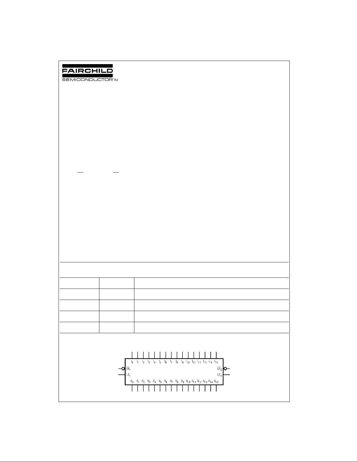
Logic Symbol
© 2000 Fairchild Semiconductor Corporation DS500354 www.fairchildsemi.com

Connection Diagram Pin Descriptions
Pin Names Description
OE
n
LE
n
I
74LVTH162373
0–I15
O
0–O15
Truth Tables
LE
1
X H X Z
H L L L
H L H H
L L X O
LE
2
X H X Z
H L L L
H L H H
L L X O
H = HIGH Voltage Level
L = LOW Voltage Level
X = Immaterial
Z = HIGH Impedance
= Previous output prior to HIGH-to-LOW transition of LE
O
o
Output Enable Input (Active LOW)
Latch Enable Input
Inputs
3-STATE Outputs
Inputs Outputs
OE
1
I0–I
7
O0–O
o
Inputs Outputs
OE
2
I8–I
15
O8–O
o
7
15
Functional Description
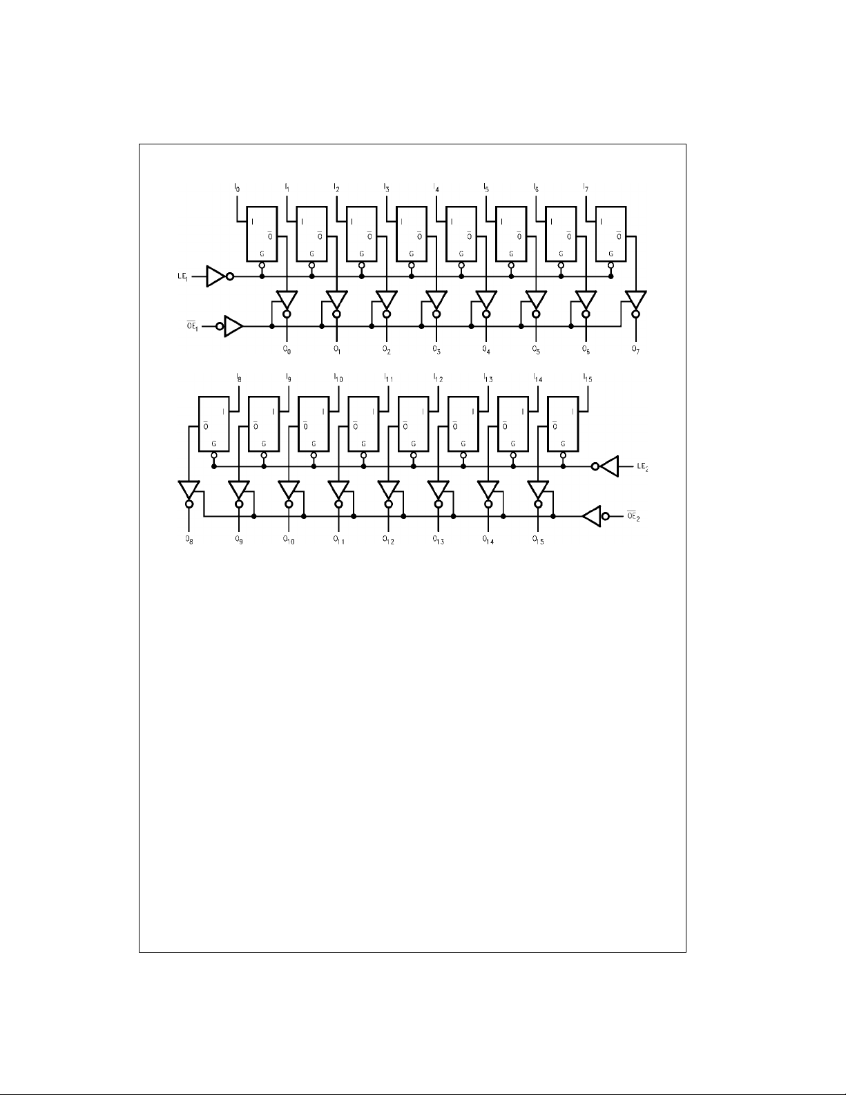
The LVTH162373 contains sixteen D-type l atches with 3- STATE standard outputs. The device is byte co ntrolled w ith each
byte functioning identically, but independent of the other. Control pins can be shorted together to obtain full 16-bit operation.
The following des cription applies to each b yte. When the Latch Enabl e (LE
latches. In this condition t he latches a re transparent, i.e, a latch output will change states each time its D input changes.
When LE
transition of LE
standard outputs are in the 2-state m ode. When OE
is LOW, the latches store information that was present on the D inputs a setup time preceding the HIGH-to-LOW
n
. The 3-STATE standard out put s are co ntrolled by the Output Enab le (OEn) input. When OEn is LOW, the
n
is HIGH, the standa rd output s are in the high impedance mode but
n
this does not interfere with entering new data into the latches.
www.fairchildsemi.com 2
) input is HIGH, da ta on the Dn enters the
n

Logic Diagrams
74LVTH162373
Please note that these diagrams are provided only for the understanding of logic operations and should not be used to estimate propagation delays .
3 www.fairchildsemi.com
 Loading...