Fairchild Semiconductor 74LVTH162245MTX, 74LVTH162245MTD, 74LVTH162245MEX, 74LVTH162245MEA, 74LVTH162245GX Datasheet

© 1999 Fairchild Semiconductor Corporation DS012446 www.fairchildsemi.com
January 1999
Revised November 1999
74L VT1 62245 • 74LVTH162245 Low V olt age 16-Bit Transceiver with 3-STA TE Outputs and 25Ω Series Resistors in
A Port Outputs
74LVT162245 • 74LVTH162245
Low Voltage 16-Bit Transceiver with 3-STATE Outputs
and 25Ω Series Resistors in A Port Outputs
General Description
The LVT162245 and LVTH162245 contains sixteen noninverting bidirectional buffers with 3-STATE outputs and is
intended for bus orien ted applications. The de vice is byte
controlled. Each byte has separate control inputs which
can be shorted toget her for full 16-bit ope ration. The T/R
inputs determine the direction of data flow through the
device. The OE
inputs disable bo th the A and B ports by
placing them in a high impedance state.
The LVT162245 and LVTH162245 are designed with
equivalent 25Ω series resistance in both the HIGH and
LOW states on the A Port outputs. This design reduces line
noise in applications such as memory address drivers,
clock drivers, and bus transceivers/transmitters.
The LVTH162245 data inputs includ e bushold, eliminat ing
the need for external pull-up resistors to hold unused
inputs.
These non-inverting transceivers are designed for low-voltage (3.3V) V
CC
applications, but with the capability to pro-
vide a TTL interface to a 5 V en vironme nt. Th e LVT162245
and LVTH162245 are fabricated with an advanced BiCMOS technology to achieve high speed operation similar to
5V ABT while maintaining a low power dissipation.
Features
■ Input and output interface ca pability to systems at 5V
V
CC
■ Bushold data inputs elimi nate th e need fo r extern al pullup resistors to hold unused inputs (74LVTH162245),
also available without bushold feat ure (74LVT162245).
■ Live insertion/extraction per mitted
■ Power Up/Down high impedance provides glitch-free
bus loading
■ A Port outputs include equivale nt series resistance of
25Ω making external termina tion resistors unnecessary
and reducing overshoot and undershoot
■ A Port outputs source/sink ±12 mA. B Port outputs
source/sink −32 mA/+64 mA
■ Functionally compatible with the 74 series 162245
■ Latch-up performance exce eds 500 mA
Ordering Code:
Note 1: Devices also available in Tape and Reel. Specif y by appending the suffix letter “X” to the ordering code.
Note 2: Use this Order Number to receive devices in Tape and Reel.
Order Number
Package
Number
Package Description
74LVT162245MEA
(Note 1)
MS48A 48-Lead Small Shrink Outline Package (SSOP), JEDEC MO-118, 0.300” Wide
74LVT162245MTD
(Note 1)
MTD48 48-Lead Thin Shrink Small Outline Package (TSSOP), JEDEC MO-153, 6.1mm Wide
74LVTH162245MEA MS48A 48-Lead Small Shrink Outline Package (SSOP), JEDEC MO-118, 0.300” Wide
[TUBE]
74LVTH162245MEX
(Note 2)
MS48A 48-Lead Small Shrink Outline Package (SSOP), JEDEC MO-118, 0.300” Wide
[TAPE and REEL]
74LVTH162245MTD MTD48 48-Lead Thin Shrink Small Outline Package (TSSOP), JEDEC MO-153, 6.1mm Wide
[TUBE]
74LVTH162245MTX
(Note 2)
MTD48 48-Lead Thin Shrink Small Outline Package (TSSOP), JEDEC MO-153, 6.1mm Wide
[TAPE and REEL]

www.fairchildsemi.com 2
74LVT162245 • 74LVTH162245
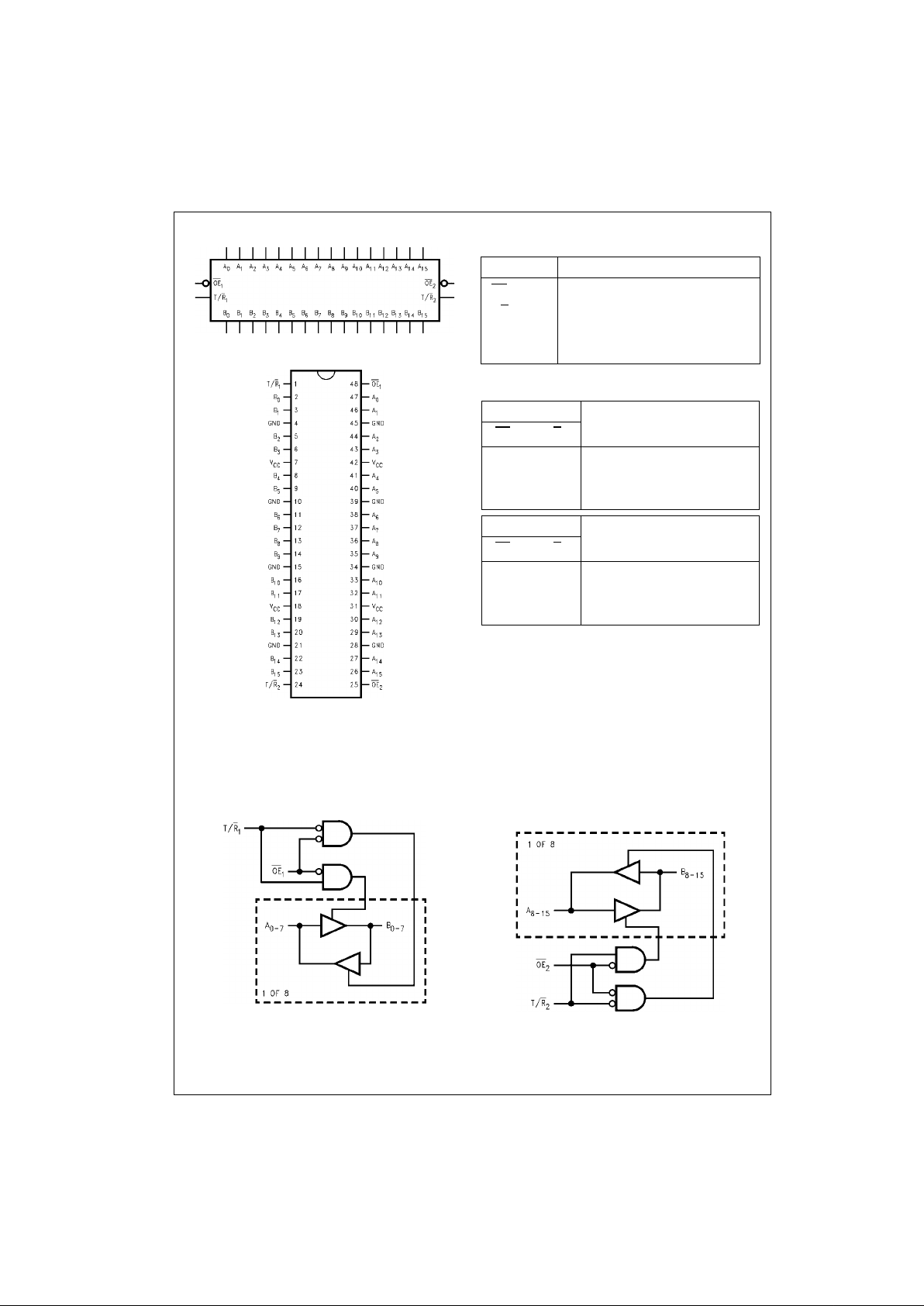
Logic Symbol
Connection Diagram
Pin Descriptions
Tr uth Tables
H = HIGH Voltage Level
L = LOW Voltage Level
X = Immaterial
Z = High Impedance
Functional Description
The LVT162245 and LVTH162245 contain sixteen non-invert ing bidir ectional b uffers with 3-S TATE outputs. The device is
byte controlled with each byte functioning identically, but independent of the other. The control pins can be shorted together
to obtain full 16-bit operation.
Logic Diagrams
Please note that these diagrams are prov ided only for the understanding of logic operations and should not be used to es t im at e propagation delays.
Pin Names Description
OE
n
Output Enable Input (Active LOW)
T/R
n
Transmit/Receive Input
A
0–A15
Side A Inputs/3-STATE Outputs
B
0–B15
Side B Inputs/3-STATE Outputs
Inputs Outputs
OE
1
T/R
1
L L Bus B0–B7 Data to Bus A0–A
7
L H Bus A0–A7 Data to Bus B0–B
7
H X HIGH-Z State on A0–A7, B0–B
7
Inputs Outputs
OE
2
T/R
2
L L Bus B8–B15 Data to Bus A8–A
15
L H Bus A8–A15 Data to Bus B8–B
15
H X HIGH-Z State on A8–A15, B8–B
15

3 www.fairchildsemi.com
74LVT162245 • 74LVTH162245
Absolute Maximum Ratings(Note 3)
Recommended Operating Conditions
Note 3: Absolute Maximum continuous ratings are those values beyond which damage to the device may occur. Exposure to these conditions or conditions
beyond those indica te d m ay adversely affect devic e reliability. Functional operation under absolute maximum rated conditions is not imp lied.
Note 4: I
O
Absolute Maximum Rating must be observed.
Symbol Parameter Value Conditions Units
V
CC
Supply Voltage −0.5 to +4.6 V
V
I
DC Input Voltage −0.5 to +7.0 V
V
O
Output Voltage −0.5 to +7.0 Output in 3-STATE
V
−0.5 to +7.0 Output in HIGH or LOW St ate (Note 4)
I
IK
DC Input Diode Current −50 VI < GND mA
I
OK
DC Output Diode Current −50 VO < GND mA
I
O
DC Output Current 64 VO > VCCOutput at HIGH State
mA
128 V
O
> VCCOutput at LOW State
I
CC
DC Supply Current per Supply Pin ±64 mA
I
GND
DC Ground Current per Ground Pin ±128 mA
T
STG
Storage Temperature −65 to +150 °C
Symbol Parameter Min Max Units
V
CC
Supply Voltage 2.7 3.6 V
V
I
Input Voltage 0 5.5 V
I
OH
HIGH-Level Output Current B Port −32
mA
A Port −12
I
OL
LOW-Level Output Current B Port 64
mA
A Port 12
T
A
Free Air Operating Temperature −40 +85 °C
∆t/∆V Input Edge Rate, V
IN
= 0.8V–2.0V, VCC = 3.0V 0 10 ns/V
 Loading...