Fairchild Semiconductor 74LVTH125SJX, 74LVTH125SJ, 74LVTH125MX, 74LVTH125MTCX, 74LVTH125MTC Datasheet
...
October 1998
Revised January 1999
74LVTH125
Low Voltage Quad Buffer with 3-STATE Outputs
74LVTH125 Low Voltage Quad Buffer with 3-STATE Outputs
General Description
The LVTH125 contains four independent non-inverting buffers with 3-STATE outputs.
These buffers are designed for low-voltage (3.3V) V
applications, but with the capability to provide a TTL inter-
face to a 5V environment. The LVTH125 is fabricated wi th
an advanced BiCMOS technology to achieve high speed
operation similar to 5V ABT while maintaining a low power
dissipation.
Features
■ Input and output interface capability to systems at 5V
V
CC
■ Bus-Hold data inputs eliminate the need for external
CC
pull-up resistors to hold unused inpu ts
■ Live insertion/extraction permitted
■ Power Up/Down high impedance provides glitch-free bus
loading
■ Outputs source/sink −32 mA/+64 mA
■ Functionally compatible with the 74 series 125
■ Latch-up performance exceeds 500 mA
Ordering Code:
Order Number Package Number Package Description
74LVTH125M M14A 14-Lead Small Outline Integrated Circuit (SOIC), JEDEC MS-120, 0.150” Narrow
74LVTH125SJ M14D 14-Lead Small Outline Package (SOP), EIAJ TYPE II, 5.3mm Wide
74LVTH125MTC MTC14 14-Lead Thin Shrink Small Outline Package (TSSOP), JEDEC MO-153, 4.4mm Wide
Device also available in Tape and Reel. Specify by appendin g s uf f ix let t er “X” to the ordering code.
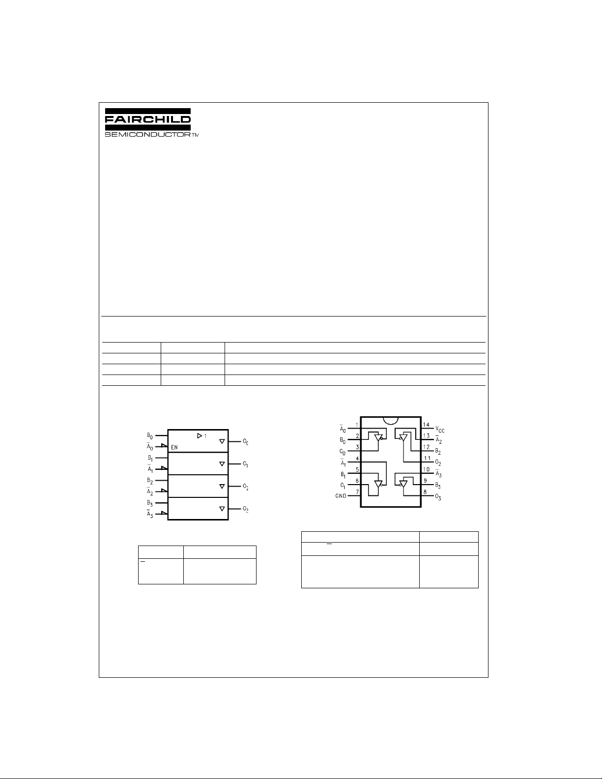
Logic Symbol
IEEE/IEC
Connection Diagram
Truth Tabl e
Pin Descriptions
Pin Names Description
, B
A
n
O
n
© 1999 Fairchild Semiconductor Corporation DS012011.prf www.fairchildsemi.com
n
Inputs
3-STATE Outputs
H = HIGH Voltage Level
L = LOW Voltage Level
X = Immaterial
Z = HIGH Impedance
Inputs Output
A
n
LLL
LHH
HXZ
B
n
O
n

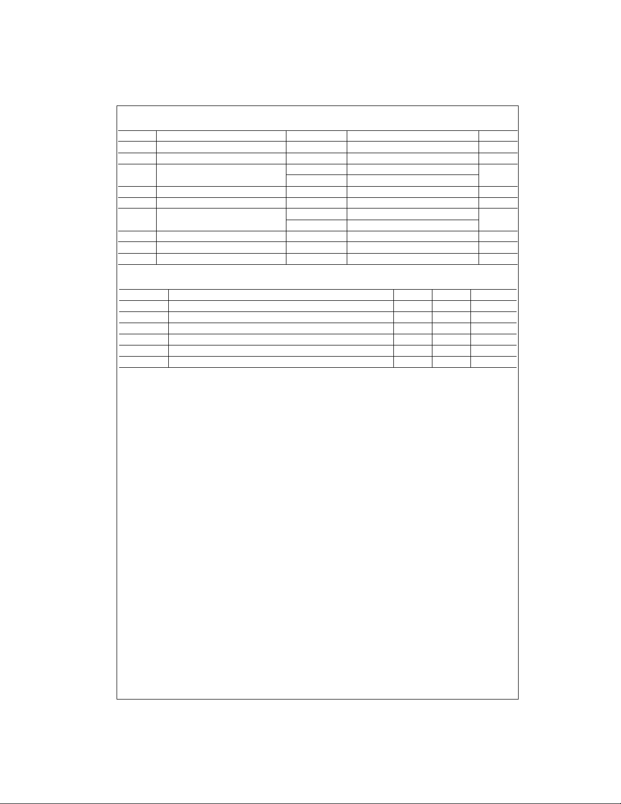
Absolute Maximum Ratings(Note 1)
Symbol Parameter Value Conditions Units
V
CC
V
I
74LVTH125
V
O
Supply Voltage −0.5 to +4.6 V
DC Input Voltage −0.5 to +7.0 V
DC Output Voltage −0.5 to +7.0 Output in 3-STATE
−0.5 to +7.0 Output in HIGH or LOW State (Note 2)
I
IK
I
OK
I
O
I
CC
I
GND
T
STG
DC Input Diode Current −50 VI < GND mA
DC Output Diode Current −50 VO < GND mA
DC Output Current 64 VO > VCCOutput at HIGH State
128 V
> VCCOutput at LOW State
O
DC Supply Current per Supply Pin ±64 mA
DC Ground Current per Ground Pin ±128 mA
Storage Temperature −65 to +150 °C
Recommended Operating Conditions
Symbol Parameter Min Max Units
V
CC
V
I
I
OH
I
OL
T
A
∆t/∆V Input Edge Rate, V
Note 1: Absolute Max imum c onti nuous ratings are thos e values beyond which da mag e to th e device may occur. Expos ure to these c ondit ions or conditions
beyond those indicated m ay ad versely affect device reliability. Functional operation under absolute maximum rate d c onditions is not implied.
Note 2: I
Supply Voltage 2.7 3.6 V
Input Voltage 0 5.5 V
HIGH Level Output Current −32 mA
LOW Level Output Current 64 mA
Free-Air Operating Temperature −40 85 °C
= 0.8V–2.0V, VCC = 3.0V 0 10 ns/V
IN
Absolute Maximum Rating must be observe d.
O
V
mA
www.fairchildsemi.com 2
 Loading...