Fairchild Semiconductor 74LVTH573WMX, 74LVTH573WM, 74LVTH573SJX, 74LVTH573SJ, 74LVTH573MTCX Datasheet
...
74LVT573 • 74LVTH573
Low Voltage Octal Transparent Latch
with 3-STAT E Outputs
74LVT573 • 74LVTH573 Low Voltage Octal T ransparent Latch with 3-STATE Outputs
March 1999
Revised March 1999
General Description
The LVT573 and LVTH573 consist of eight latc hes with 3STAT E ou tpu ts for bus organized system ap pli ca tions. The
latches appear transpar ent to the dat a when Latch Ena ble
(LE) is HIGH. When LE is low, the data sa tisfying the inp ut
timing requirements is latched. Data appears on th e bus
when the Output Enable (OE
the bus output is in the high impedance state.
The LVTH573 data inputs include b ushold, eliminati ng the
need for external pull-up resistors to hold unused inputs.
These octal latches are designed for low-voltage (3.3V)
applications, but with the capability to provide a TTL
V
CC
interface to a 5V environme nt. The LVT573 and LVTH573
are fabricated with an advanced BiCMOS technology to
) is LOW. When OE is HIGH,
achieve high speed operation similar to 5V ABT while
maintaining a low power dissipation.
Features
■ Input and output interface capability to systems at
5V V
CC
■ Bushold data inputs elimina te the nee d for exte rnal pullup resistors to hold unused inputs (74LVTH573), also
available without bushold feature (74LVT573).
■ Live insertion/extraction per mitt ed
■ Power Up/Down high impedance provides glitch-free
bus loading
■ Outputs source/sink −32 mA/+64 mA
■ Functionally compatible with the 74 series 573
■ Latch-up performance exce eds 500 mA
Ordering Code:
Order Number Package Number Package Description
74LVT573WM M20B 20-Lead Small Outline Integrated Circuit (SOIC), JEDEC MS-013, 0.300” Wide
74LVT573SJ M20D 20-Lead Small Outline Package (SOP), EIAJ TYPE II 5.3mm Wide
74LVT573MTC MTC20 20-Lead Thin Shrink Small Outline Package (TSSOP), JEDEC MO-153, 4.4mm Wide
74LVT573MSA MSA20 20-Lead Shrink Small Outline Package (SSOP), EIAJ TYPE II, 5.3mm Wide
74LVTH573WM M20B 20-Lead Small Outline Integrated Circuit (SOIC), JEDEC MS-013, 0.300” Wide
74LVTH573SJ M20D 20-Lead Small Outline Package (SOP), EIAJ TYPE II 5.3mm Wide
74LVTH573MTC MTC20 20-Lead Thin Shrink Small Outline Package (TSSOP), JEDEC MO-153, 4.4mm Wide
74LVTH573MSA MSA20 20-Lead Shrink Small Outline Package (SSOP), EIAJ TYPE II, 5.3mm Wide
Device also available in Tape and Reel. Specify by appending s uffix let te r “X” to the ordering code.
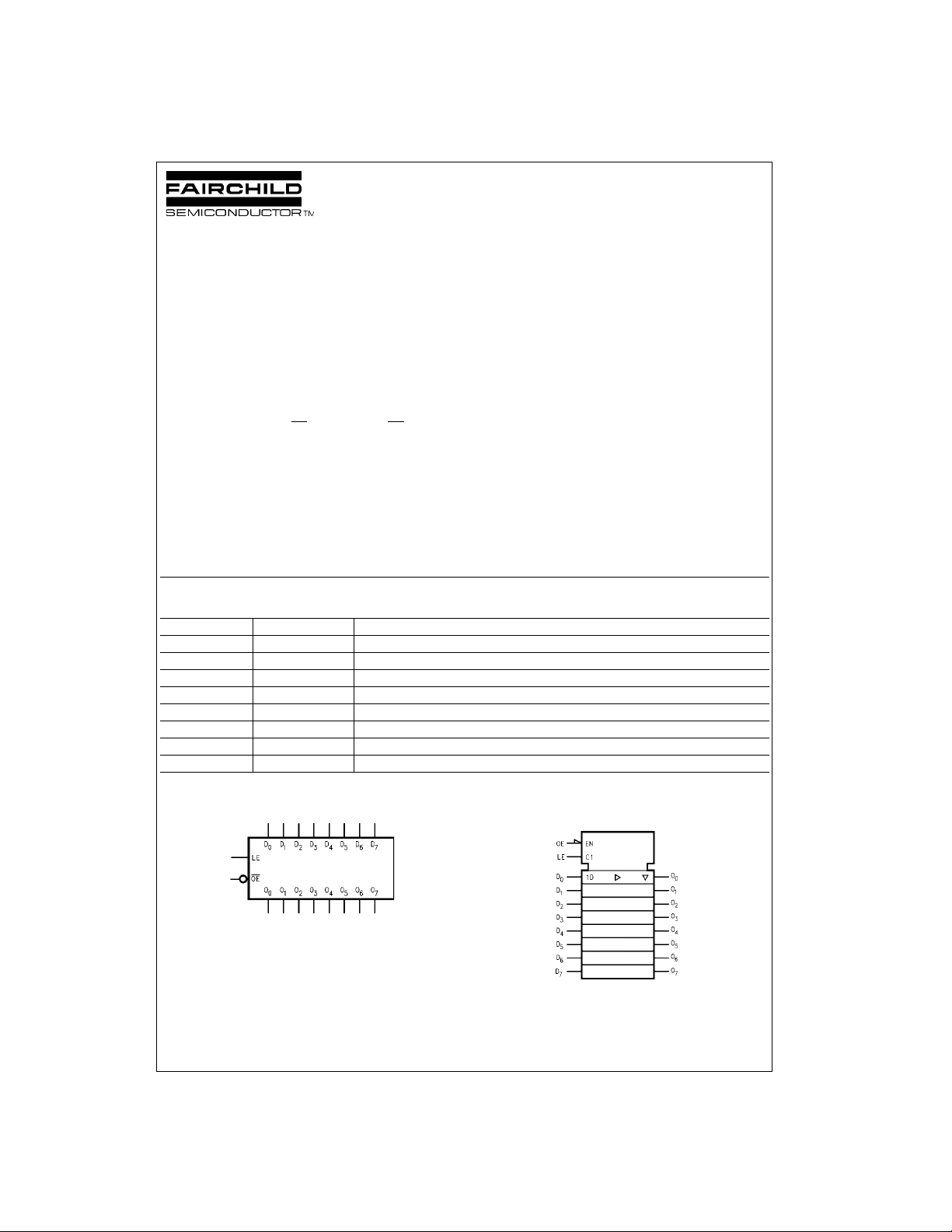
Logic Symbols
IEEE/IEC
© 1999 Fairchild Semiconductor Corporation DS012450.prf www.fairchildsemi.com

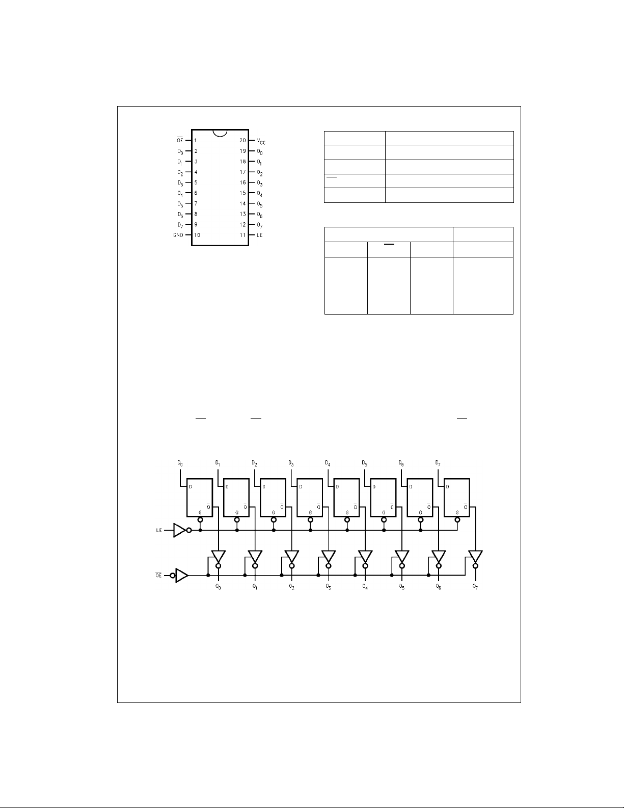
Connection Diagram Pin Descriptions
Pin Names Description
D
0–D7
LE Latch Enable Input
OE
O
0–O7
Data Inputs
Output Enable Input
3-STATE Latch Outputs
74LVT573 • 74LVTH573
Truth Table
Inputs Outputs
LE OE
D
n
XHX Z
HLL L
HLH H
LLX O
H = HIGH Voltage Level
L = LOW Voltage Level
Z = High Impedance
X = Immaterial
= Previous O0 before HIGH to LOW transition of Latch Enable
O
0
Functional Description
The LVT573 and LVTH573 contain eight D-type latches with 3-STATE standard outputs. When the Latch Enable (LE) input
is HIGH, data on the D
change state eac h ti me its D-typ e inpu t chan ges. W hen LE is LOW, the latch es stor e the inform ation t hat was pr esent on
the D-type inputs a setup time preceding the HIGH-to- LOW tra nsition of LE . The 3-STATE standard outputs are controlled
by the Output Enable (OE
standard outputs are in the high impedance mode but this does not interfere with entering new data into the latches.
inputs enters the latches. In this condition the latches are transparent, i.e., a latch output will
n
) input. When OE is LOW, the standard outputs are in the 2-state mode. Wh en OE is HIGH, the
Logic Diagram
O
n
0
Please note that this diagram is provided only f or t he understanding of logic operations and should not be used to estimate propagation delays.
www.fairchildsemi.com 2

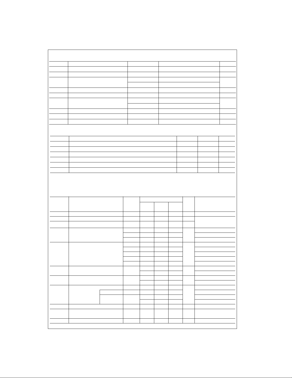
Absolute Maximum Ratings(Note 1)
Symbol Parameter Value Conditions Units
V
CC
V
I
V
O
Supply Voltage −0.5 to +4.6 V
DC Input Voltage −0.5 to +7.0 V
DC Output Voltage −0.5 to +7.0 Output in 3-STATE
−0.5 to +7.0 Output in High or Low State (Note 2)
I
IK
I
OK
I
O
I
CC
I
GND
T
STG
DC Input Diode Current −50 VI < GND mA
DC Output Diode Current −50 VO < GND mA
DC Output Current 64 VO > VCCOutput at High State
128 V
> VCCOutput at Low State
O
mA
DC Supply Current per Supply Pin ±64 mA
DC Ground Current per Grou nd Pin ±128 mA
Storage Temperature −65 to +150 °C
Recommended Operating Conditions
Symbol Parameter Min Max Units
V
CC
V
I
I
OH
I
OL
T
A
∆t/∆V Input Edge Rate, V
Note 1: Absolute Maximum continuous ratings are those values beyond which damage to the device may occur. Exposure to these conditions or conditions
beyond those indica te d m ay adversely affect devic e reliability. Functional operation under absolute maximum rated conditions is not imp lied.
Note 2: I
Supply Voltage 2.7 3.6 V
Input Voltage 0 5.5 V
High-Level Output Current −32 mA
Low-Level Output Current 64 mA
Free-Air Operating Temperature −40 85 °C
= 0.8V–2.0V, VCC = 3.0V 0 10 ns/V
IN
Absolute Maximum Rating must be observed.
O
74LVT573 • 74LVTH573
V
DC Electrical Characteristics
Symbol Parameter
V
IK
V
IH
V
IL
V
OH
V
OL
I
I(HOLD)
(Note 4)
I
I(OD)
(Note 4)
I
I
I
OFF
I
PU/PD
I
OZL
Input Clamp Diode Voltage 2.7 −1.2 V II = −18 mA
Input HIGH Voltage 2.7–3.6 2.0 V VO ≤ 0.1V or
Input LOW Voltage 2.7–3.6 0.8 V
Output HIGH Voltage 2.7–3.6 VCC − 0.2
Output LOW Voltage 2.7 0.2
Bushold Input Minimum Drive 3.0 75
Bushold Input Over-Drive 3.0 500
Current to Change State −500 (Note 6)
Input Current 3.6 10
Control Pins 3.6 ±1V
Data Pins 3.6 −5V
Power Off Leakage Current 0 ±100 µA0V ≤ VI or VO ≤ 5.5V
Power up/down 3-STATE 0–1.5V ±100 µAVO = 0.5V to 3.0V
Output Current VI = GND or V
3-STATE Output Leakage Current 3.6 −5 µAVO = 0.5V
V
CC
(V)
2.7 2.4 IOH = −8 mA
3.0 2.0 IOH = −32 mA
2.7 0.5 IOL = 24 mA
3.0 0.4 IOL = 16 mA
3.0 0.5 IOL = 32 mA
3.0 0.55 IOL = 64 mA
T A = −40°C to +85°C
Min Typ Max
(Note 3)
−75 VI = 2.0V
Units Conditions
VO ≥ VCC − 0.1V
IOH = −100 µA
V
IOL = 100 µA
V
VI = 0.8V
µA
(Note 5)
µA
VI = 5.5V
= 0V or V
I
µA
= 0V
1V
I
= V
I
CC
CC
CC
3 www.fairchildsemi.com
 Loading...