Fairchild Semiconductor 74LVT374MTC, 74LVT374WMX, 74LVT374WM, 74LVT374SJX, 74LVT374SJ Datasheet
...
© 1999 Fairchild Semiconductor Corporation DS012016 www.fairchildsemi.com
September 1999
Revised October 1999
74LVT374 • 74LVTH374 Low Voltage Octal D-Type Flip-Flop with 3-STATE Outputs
74LVT374 • 74LVTH374
Low Voltage Octal D-Type Flip-Flop
with 3-STATE Outputs
General Description
The LVT374 and LVTH374 are high-speed, low-power
octal D-type flip-flop s featuring separat e D-type inputs f or
each flip-flop and 3- STATE outputs for bus-o riented applications. A buffered Clock (CP) and Output Enable (OE
) are
common to all flip-flops.
The LVTH374 data inputs include bush old, eliminati ng the
need for external pull-up resistors to hold unused inputs.
These octal flip-flops are designed for low-voltage (3.3V )
V
CC
applications, but with the capability to provide a TTL
interface to a 5V environme nt. The LVT374 and LVTH374
are fabricated with an advanced BiCMOS technology to
achieve high speed operation similar to 5V ABT while
maintaining low power dissipation.
Features
■ Input and output interface capability to systems at
5V V
CC
■ Bus-Hold data inputs eliminate the need for external
pull-up resistors to hold unused inputs (74LVTH374),
also available without bushold feature (74LVT374).
■ Live insertion/extraction per mitt ed
■ Power Up/Down high impedance provides glitch-free
bus loading
■ Outputs source/sink −32 mA/+64 mA
■ Functionally compatible with the 74 series 374
■ Latch-up performance exceeds 500 mA
Ordering Code:
Device also available in Tape and Reel. Specify by appending s uffix let te r “X” to the ordering code.
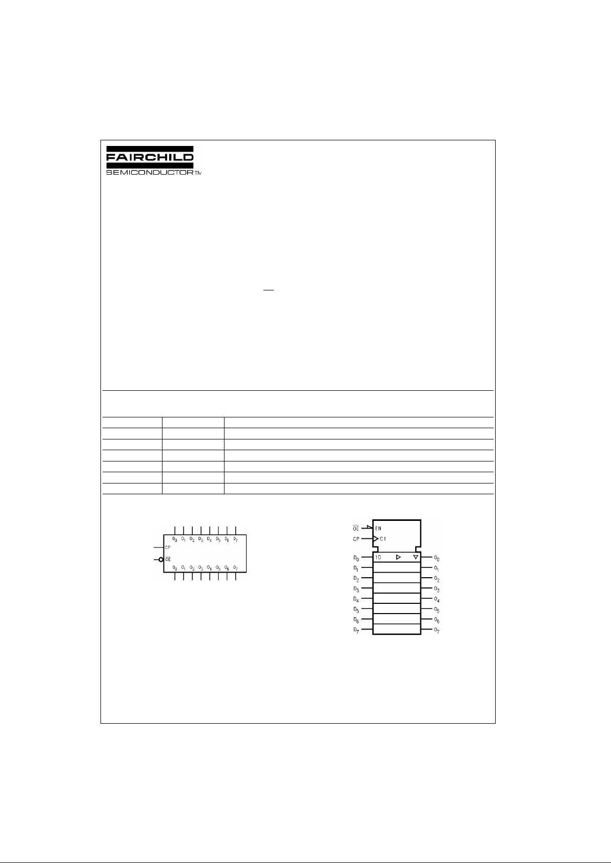
Logic Symbols
IEEE/IEC
Order Number Package Number Package Description
74LVT374WM M20B 20-Lead Small Outline Integrated Circuit (SOIC), JEDEC MS-013, 0.300” Wide
74LVT374SJ M20D 20-Lead Small Outline Package (SOP), EIAJ TYPE II, 5.3mm Wide
74LVT374MTC MTC20 20-Lead Thin Shrink Small Outline Package (TSSOP), JEDEC MO-153, 4.4mm Wide
74LVTH374WM M20B 20-Lead Small Outline Integrated Circuit (SOIC), JEDEC MS-013, 0.300” Wide
74LVTH374SJ M20D 20-Lead Small Outline Package (SOP), EIAJ TYPE II, 5.3mm Wide
74LVTH374MTC MTC20 20-Lead Thin Shrink Small Outline Package (TSSOP), JEDEC MO-153, 4.4mm Wide

www.fairchildsemi.com 2
74LVT374 • 74LVTH374
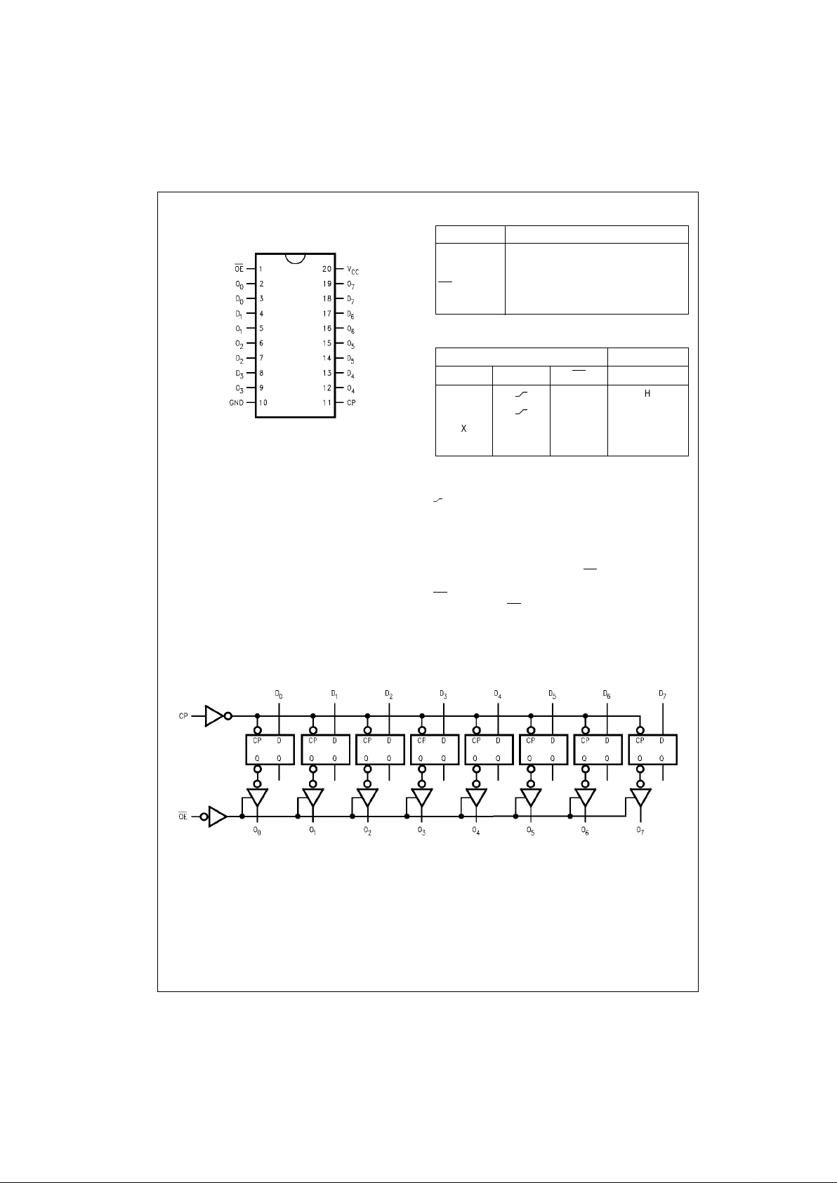
Connection Diagram Pin Descriptions
Tr uth Table
H = HIGH Voltage Level
L = LOW Voltage Level
X = Immaterial
Z = High Impedance
= LOW-to-HIGH Transition
O
o
= Previous Oo before HIGH-to-LOW of CP
Functional Description
The LVT374 and LVTH374 consist of eigh t edge-trigg ered
flip-flops with individual D-type inputs and 3-STATE true
outputs. The buffered c lock and buffered Output Enable
are common to all flip-flops. The eight flip-flops will store
the state of their individual D inputs that meet the setup and
hold time requiremen ts on the LOW-to-HIGH Clock (CP)
transition. With the Output Enable (O E
) LOW, the contents
of the eight flip-flops are available at the outputs. When the
OE
is HIGH, the outputs go to the high impedance state.
Operation of the O E
input does not affect the state of the
flip-flops.
Logic Diagram
Please note that this diagram is provided o nly f or t he understanding of lo gic operations and should not be used to estimate propagation delays.
Pin Names Description
D
0–D7
Data Inputs
CP Clock Pulse Input
OE
3-STATE Output Enable Input
O
0–O7
3-STATE Outputs
Inputs Outputs
D
n
CP OE O
n
H
LH
L
LL
XLL O
o
XXH Z

3 www.fairchildsemi.com
74LVT374 • 74LVTH374
Absolute Maximum Ratings (Note 1)
Recommended Operating Conditions
Note 1: Absolute Maximum continuous ratings are those values beyond which damage to the device may occur. Exposure to these conditions or conditions
beyond those indica te d m ay adversely affect dev ic e reliability. Functional operation under absolute maxim um rated conditions is not imp lied.
Note 2: I
O
Absolute Maximum Rating must be observed.
Symbol Parameter Value Conditions Units
V
CC
Supply Voltage −0.5 to +4.6 V
V
I
DC Input Voltage −0.5 to +7.0 V
V
O
DC Output Voltage −0.5 to +7.0 Output in 3-STATE V
−0.5 to +7.0 Output in HIGH or LOW State (Note 2) V
I
IK
DC Input Diode Current −50 VI < GND mA
I
OK
DC Output Diode Current −50 VO < GND mA
I
O
DC Output Current 64 VO > VCCOutput at HIGH State
mA
128 V
O
> VCCOutput at LOW State
I
CC
DC Supply Current per Supply Pin ±64 mA
I
GND
DC Ground Cu rrent per Ground Pin ±128 mA
T
STG
Storage Temperature −65 to +150 °C
Symbol Parameter Min Max Units
V
CC
Supply Voltage 2.7 3.6 V
V
I
Input Voltage 0 5.5 V
I
OH
HIGH-Level Output Current −32 mA
I
OL
LOW-Level Output Current 64 mA
T
A
Free-Air Operating Temperature −40 85 °C
∆t/∆V Input Edge Rate, V
IN
= 0.8V–2.0V, VCC = 3.0V 0 10 ns/V
 Loading...