

Fairchild Semiconductor 74LVT32374 Datasheet
74LVT32374 • 74LVTH32374
Low Voltage 32-Bit D-Type Flip-Flop
with 3-STATE Outputs
74LVT32374 • 74LVTH32374 Low Voltage 32-Bit D-Type Flip-Flop with 3-STATE Outputs
April 2001
Revised June 2002
General Description
The LVT32374 and LVTH32374 contain thirty-two noninverting D-type flip-flops with 3-STATE outputs and are
intended for bus orien ted applications. The de vice is byte
controlled. A buffered clock ( CP) and Output Ena ble (OE
are common to each byte and can be sho rted togethe r for
full 32-bit operation.
The LVTH32374 data inputs includ e bushold, eliminating
the need for external pull-up resistors to hold unused
inputs.
These flip-flops are designed for low-voltage (3.3V) V
applications, but with the capability to provide a TTL inter-
face to a 5V environment. Th e LVT32374 and LVTH32374
are fabricated with an advanced BiCMOS technology to
achieve high speed operation similar to 5V ABT while
maintaining a low power dissipation.
Features
■ Input and output interface capability to systems at
5V V
CC
■ Bushold data inputs eliminate the need for external
)
pull-up resistors to hold unused inputs (74LVTH32374)
■ Also available without bushold feature (74LVT32374)
■ Live insertion/extraction per mi tt ed
■ Power Up/Down high impedance provides glitch-free
bus loading
■ Outputs source/sink
CC
■ ESD performance:
Human-body model
Machine model
Charged-device model
■ Packaged in plastic Fine-Pitch Ball Grid Array (FBGA)
> 200V
Ordering Code:
Order Number
74LVT32374G
(Note 1)(Note 2)
74LVTH32374G
(Note 1)(Note 2)
Note 1: Ordering code “G” indicates Trays.
Note 2: Devices also available in Tape and Reel. Specify by appending th e s uffix let t er “X” to the ordering code.
Package
Number
BGA96A
(Preliminary)
BGA96A 96-Ball Fine-Pitch Ball Grid Array (FBGA), JEDEC MO-205, 5.5mm Wide
96-Ball Fine-Pitch Ball Grid Array (FBGA), JEDEC MO-205, 5.5mm Wide
Package Description
Logic Symbol
−32 mA/+64 mA
> 2000V
> 1000V
© 2002 Fairchild Semiconductor Corporation DS500452 www.fairchildsemi.com

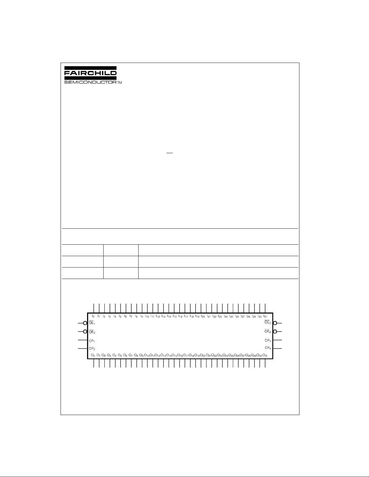
Connection Diagram
74LVT32374 • 74LVTH32374
(Top Thru View)
Pin Descriptions
Pin Names Description
OE
CP
I
0–I31
O
0–O31
n
n
Output Enable Input (Active LOW)
Clock Pulse Input
Inputs
3-STATE Outputs
FBGA Pin Assignments
123456
A O
B O
C O
D O
E O
F O
G O
H O
J O
K O
L O
M O
N O
P O
R O
T O
O0OE1CP
1
O2GND GND I
3
O4V
5
7
9
11
13O12
14O15
17O16
19O18
21O20VCC2VCC2I20
23O22
25O24
27O26VCC2VCC2I26
29O28
30O31
CC1VCC1I4
O6GND GND I
O8GND GND I
O10V
CC1VCC1I10
GND GND I
OE2CP2I
OE3CP3I
GND GND I
GND GND I
GND GND I
GND GND I
OE4CP4I
1I0
I
1
I
2
3
I
5
I
6
7
I
8
9
I
11
I
12
13
I
15
14
I
16
17
I
18
19
I
21
I
22
23
I
24
25
I
27
I
28
29
I
31
30
Functional Description
The LVT32374 and LVTH32374 consist of thirty-two edge-triggered flip-flops with individual D-type inputs and 3-STATE true
outputs. The device i s byte con troll ed with each byte function ing id entic ally, but independent of the ot her. The control pins
can be shorted together to obtain full 32-bit operation. Each byte has a buffered clock and buffered Output Enable common
to all flip-flops w ithi n that byte . T he des cri pt ion which follows appl ies to ea ch b yte. Each flip-flop w ill s tor e th e sta te of their
individual D-type in puts tha t meet the setup an d hold time requi rements o n the LOW- to-HIGH Cl ock (CP
the Output Enable (OE
to the high impedance state. Operation of the OE
) LOW, the contents of the flip-flops are available at the outputs. When OEn is HIGH, the outputs go
n
input does not affect the state of the flip-flops.
n
) transition. With
n
Truth Tables
Inputs Outputs Inputs Outputs
CP
1
LL X O
XH X Z XHX Z
CP
3
LL X O
XH X Z XHX Z
H = HIGH Voltage Level
L = LOW Voltage Level
X = Immaterial
www.fairchildsemi.com 2
OE
1
LH H
LL L
I0–I
7
O0–O
7
o
CP
2
LLX O
OE
I8–I
2
15
O8–O
LH H
LL L
o
Inputs Outputs Inputs Outputs
OE
3
LH H
LL L
I16–I
23
O16–O
23
o
CP
4
OE
I24–I
4
31
LH H
LL L
LLX O
Z = HIGH Impedance
= Previous Oo before HIGH-to-LOW of CP
O
o
O24–O
o
15
31
 Loading...