Fairchild Semiconductor 74LVTH32373, 74LVT32373 Datasheet

74LVT32373 • 74LVTH32373
Low Voltage 32-Bit Transparent Latch
with 3-STATE Outputs (Preliminary)
Preliminary
74LVT32373 • 74LVTH32373 Low Voltage 32-Bit Transparent Latch with 3-STATE Outputs (Preliminary)
August 2001
Revised August 2001
General Description
The LVT32373 and LVTH32373 contain thirty-two noninverting latches with 3- STATE outputs and are i ntended
for bus oriented applications. The d evice is byte controlled.
The flip-flops appear transparent to the data when the
Latch Enable (LE) is HIGH. When LE is LOW, the data that
meets the setup time is latched. Dat a appears on the bus
when the Output Enable (OE
the outputs are in a high impedance state.
The LVTH32373 data inputs includ e bushold, eliminating
the need for external pull-up resistors to hold unused
inputs.
These latches are designed for low-voltage (3.3V) V
applications, but with the capability to provide a TTL inter-
face to a 5V environment. Th e LVT32373 and LVTH32373
are fabricated with an advanced BiCMOS technology to
achieve high speed operation similar to 5V ABT while
maintaining a low power dissipation.
) is LOW. When OE is HIGH,
Features
■ Input and output interface capability to systems at
5V V
CC
■ Bushold data inputs eliminate the need for external
pull-up resistors to hold unused inputs (74LVTH32373),
also available without bushold feat ure (74LVT32373)
■ Live insertion/extraction per mi tt ed
■ Power Up/Down high impedance provides glitch-free
bus loading
■ Outputs source/sink
■ ESD performance:
CC
Human-body model
Machine model
Charged-device model
■ Packaged in plastic Fine-Pitch Ball Grid Array (FBGA)
(Preliminary)
−32 mA/+64 mA
> 2000V
> 200V
Ordering Code:
Order Number Package Number Package Descript io n
74LVT32373GX
(Note 1)
74LVTH32373GX
(Note 1)
Note 1: BGA package available in Tape and Reel only.
BGA96A
(Preliminary)
BGA96A
(Preliminary)
96-Ball Fine-Pitch Ball Grid Array (FBGA), JEDEC MO-205, 5.5mm Wide
[TAPE and REEL]
96-Ball Fine-Pitch Ball Grid Array (FBGA), JEDEC MO-205, 5.5mm Wide
[TAPE and REEL]
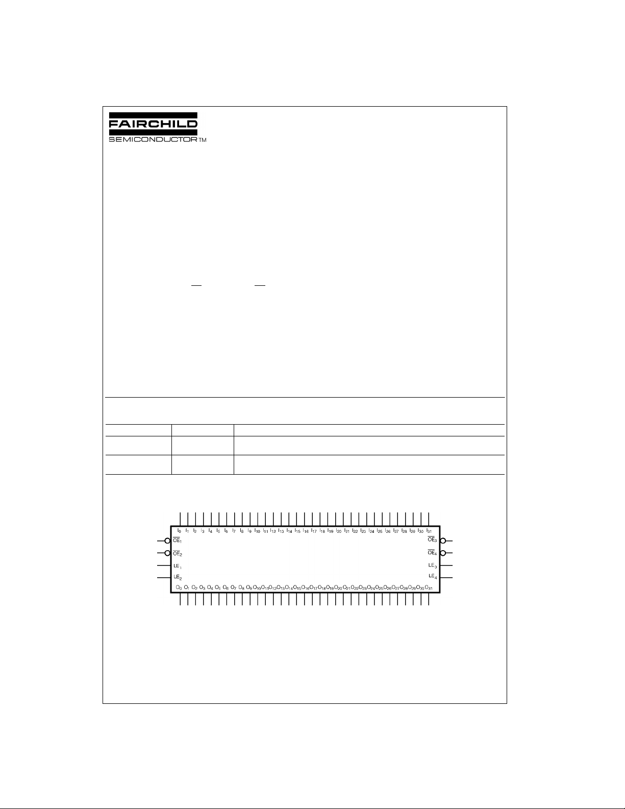
Logic Symbol
> 1000V
© 2001 Fairchild Semiconductor Corporation DS500548 www.fairchildsemi.com

Preliminary
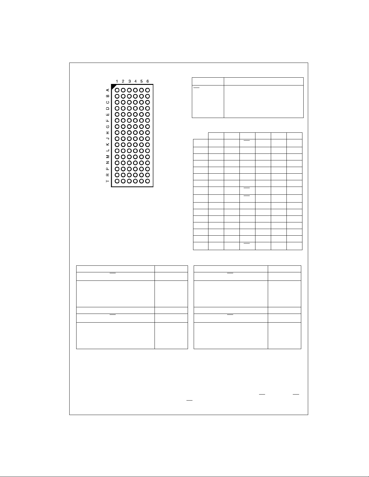
Connection Diagram
74LVT32373 • 74LVTH32373
(Top Thru View)
Pin Descriptions
Pin Names Description
OE
LE
I
0–I31
O
0–O31
n
n
Output Enable Input (Active LOW)
Latch Enable Input
Inputs
3-STATE Outputs
FBGA Pin Assignments
123456
A O
B O
C O
D O
E O
F O
G O
H O
J O
K O
L O
M O
N O
P O
R O
T O
O0OE1LE
1
O2GND GND I
3
O4V
5
7
9
11
13O12
14O15
17O16
19O18
21O20VCC2VCC2I20
23O22
25O24
27O26VCC2VCC2I26
29O28
30O31
CC1VCC1I4
O6GND GND I
O8GND GND I
O10V
CC1VCC1I10
GND GND I
OE2LE2I
OE3LE3I
GND GND I
GND GND I
GND GND I
GND GND I
OE4LE4I
1I0
I
1
I
2
3
I
5
I
6
7
I
8
9
I
11
I
12
13
I
15
14
I
16
17
I
18
19
I
21
I
22
23
I
24
25
I
27
I
28
29
I
31
30
Truth Table
Inputs Outputs Inputs Outputs
CP
1
OE
1
I0–I
7
O0–O
7
CP
2
OE
I8–I
2
15
O8–O
15
XH X Z XHX Z
HL L L HLL L
HL H H HLH H
LL X O
0
LLX O
0
Inputs Outputs Inputs Outputs
CP
3
OE
3
I16–I
23
O16–O
23
CP
4
OE
I24–I
4
31
O24–O
31
XH X Z XHX Z
HL L L HLL L
HL H H HLH H
LL X O
H = HIGH Voltage Lev el L = LOW Voltage Level X = Immaterial Z = HIGH Impedan ce Oo = Previous Oo prior to HIGH- to -LO W tr ans iti on of LE
0
LLX O
0
Functional Description
The LVT32373 and LVTH32373 contain thirty-two D-type latche s with 3-STATE standard outputs. The device is byte controlled with each byte functioning identically, but independent of the other. Control pins can be shorted together to obtain full
32-bit opera t i on. Th e f o ll o wi ng de s c rip t ion a pp l ie s to ea c h byt e. Wh en t he Lat c h En a ble ( LE
enters the latches. In this condition the latches are transparent, i.e, a latch output will change states each time its D input
changes. When LE
HIGH-to-LOW transition of LE
is LOW, the latches store information that was present on the D inputs a setup time preceding the
n
. The 3-STA TE standard outputs are controlled by the Output Enable (OEn) input. When OE
n
is LOW, the standard outputs are in the 2-state mode. When O En is HIGH, the standard outputs are in the high impedance
mode but this does not interfere with entering new data into the latches.
www.fairchildsemi.com 2
) input is HIGH, data on the D
n
n
n
 Loading...