Fairchild Semiconductor 74LVT16374MTDX, 74LVT16374MTD, 74LVT16374MEAX, 74LVT16374MEA Datasheet

January 1999
Revised April 1999
74LVT16374 • 74LVTH16374 Low Voltage 16-Bit D-Type Flip-Flop with 3-STATE Outputs
© 1999 Fairchild Semiconductor Corporation DS012022.prf www.fairchildsemi.com
74LVT16374 • 74LVTH16374
Low Voltage 16-Bit D-Type Flip-Flop with
3-STATE Outputs
General Description
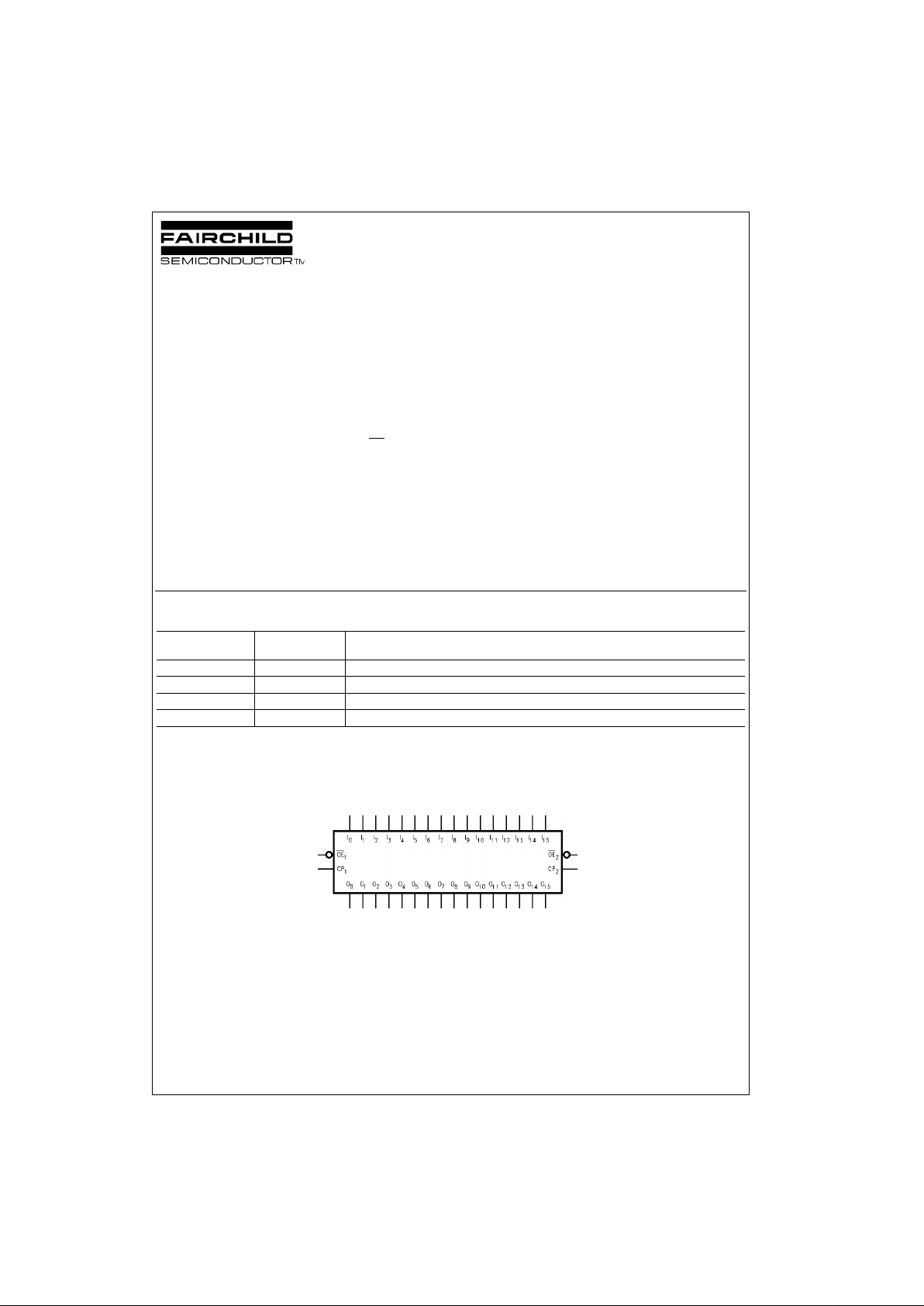
The LVT16374 and LVTH16374 contain sixteen non-inverting D-type flip-flops with 3-STATE outputs and is intended
for bus oriented applications. The device is byte controlled.
A buffered clock (CP) and Output Enable ( OE
) are common to each byte and can be shorted together for full 16-bit
operation.
The LVTH16374 data inputs includ e bushold, eliminating
the need for external pull-up resistors to hold unused
inputs.
These flip-flops are de signed for low-voltage (3.3V) V
CC
applications, but with the capability to provide a TTL interface to a 5V environment. Th e LVT16374 and LVTH16374
are fabricated with an advanced BiCMOS technology to
achieve high speed operation similar to 5V ABT while
maintaining a low power dissipation.
Features
■ Input and output interface capa bility to systems at 5V
V
CC
■ Bushold data inputs elimina te the nee d for exte rnal pul lup resistors to hold unused inputs (74LVTH16374), also
available without bushold feature (74LVT16374).
■ Live insertion/extraction per mitt ed
■ Power Up/Down high impedance provides glitch-free
bus loading
■ Outputs source/sink −32 mA/+64 mA
Ordering Code:
Device also available in Tape and Reel. Specify by appending s uffix let te r “X” to the ordering code.
Logic Symbol
Order Number Package
Number
Package Descript ion
74LVT16374MEA MS48A 48-Lead Small Shrink Outline Package (SSOP), JEDEC MO-118, 0.300” Wide
74LVT16374MTD MTD48 48-Lead Thin Shrink Small Outline Package (TSSOP), JEDEC MO-153, 6.1mm Wide
74LVTH16374MEA MS48A 48-Lead Small Shrink Outline Package (SSOP), JEDEC MO-118, 0.300” Wide
74LVTH16374MTD MTD48 48-Lead Thin Shrink Small Outline Package (TSSOP), JEDEC MO-153, 6.1mm Wide

www.fairchildsemi.com 2
74LVT16374 • 74LVTH16374
Connection Diagram Pin Descriptions
Tr uth Tables
H = HIGH Voltage Level
L = LOW Voltage Level
X = Immaterial
Z = HIGH Impedance
O
o
= Previous Oo before HIGH to LOW of CP
Functional Description
The LVT16374 and LVTH16374 consist of sixteen edge -trigge red flip- flop s with in dividual D-type inputs a nd 3-S TATE true
outputs. The device is byt e contro lled wi th eac h byte fun ctioni ng ident ically, but independe nt of the o ther. The control pins
can be shorted together to obtain full 16-bit operation. Each byte has a buffered clock and buffered Output Enable common
to all flip-flops wit hin that byte . T he description which follows app l ies to ea ch b yte. Each flip-flop will s tor e th e sta te of th eir
individual D-type input s that meet the setup an d hold time require ments o n the LOW-to- HIGH Cl ock (CP
n
) transition. With
the Output Enable (OE
n
) LOW, the contents of the flip-flops are available at the outputs. When OEn is HIGH, the outputs go
to the high impedance state. Operation of the OE
n
input does not affect the state of the flip-flops.
Pin Names Description
OE
n
Output Enable Input (Active LOW)
CP
n
Clock Pulse Input
I
0–I15
Inputs
O
0–O15
3-STATE Outputs
Inputs Outputs
CP
1
OE
1
I0–I
7
O0–O
7
LH H
LL L
LL X O
o
XH X Z
Inputs Outputs
CP
2
OE
2
I8–I
15
O8–O
15
LH H
LL L
LL X O
o
XH X Z

3 www.fairchildsemi.com
74LVT16374 • 74LVTH16374
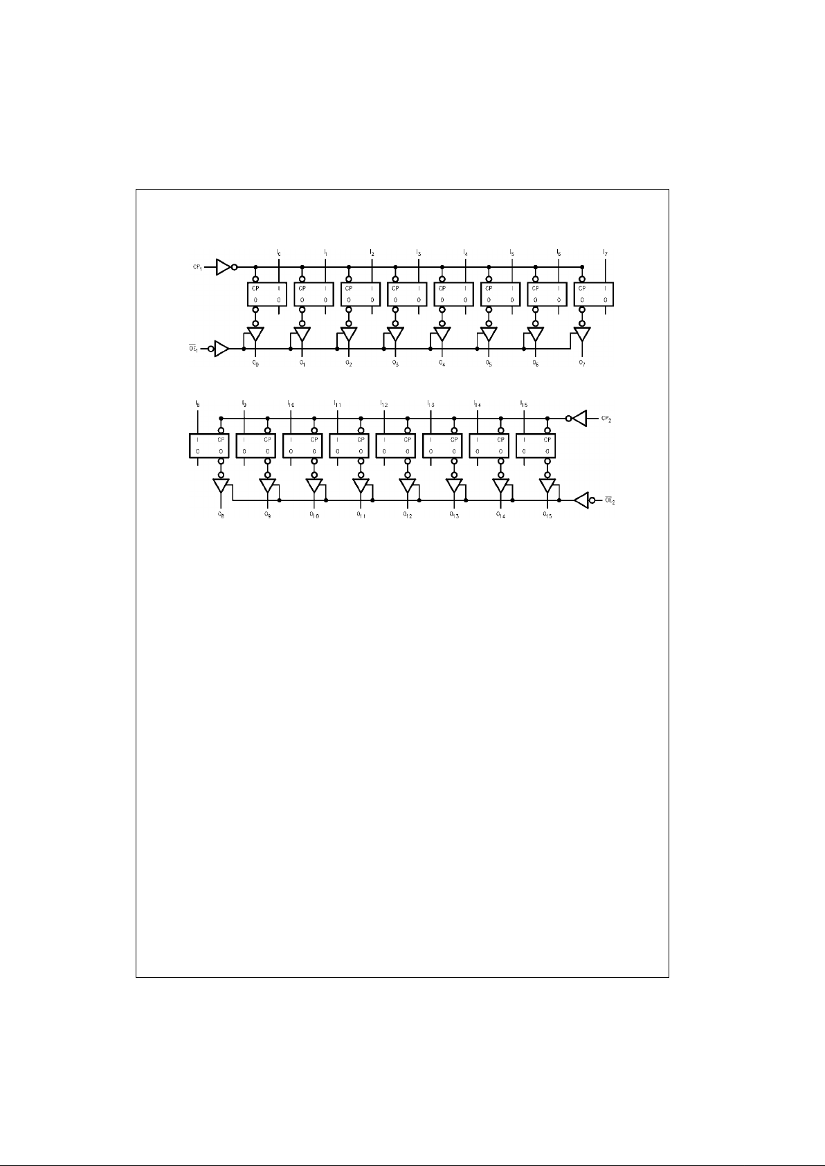
Logic Diagrams
Byte 1 (0:7)
Byte 2 (8:15)
Please note that thes e diagrams are provided f or t he understanding of logic operaiton and should not be used to estimate prop agation delays.
 Loading...