Fairchild Semiconductor 74LVTH16373MTDX, 74LVTH16373MTD, 74LVTH16373MEAX, 74LVTH16373MEA, 74LVT16373MTDX Datasheet
...
74LVT16373 • 74LVTH16373
Low Voltage 16-Bit Transparent Latch with
3-STATE Outputs
74LVT16373 • 74LVTH16373 Low Voltage 16-Bit Transparent Latch with 3-STATE Outputs
January 1999
Revised April 1999
General Description
The LVT16373 and LVTH16373 contain sixteen non-inverting latches with 3-STATE outputs and is intended for bus
oriented applications. The device is byte controlled. The
flip-flops appear t ransparent to the data when the Latch
Enable (LE) is HIGH. When LE is LOW, the data that meets
the setup time is l atched. Data appe ars on the bus wh en
the Output Enable (OE
outputs are in a high impedance state.
The LVTH16373 data inputs includ e bushold, eliminating
the need for external pull-up resistors to hold unused
inputs.
These latches are designed for low-voltage (3.3V) V
applications, but with the capability to provide a TTL inter-
face to a 5V environment. Th e LVT16373 and LVTH16373
are fabricated with an advanced BiCMOS technology to
) is LOW. When OE is HIGH, the
achieve high speed operation similar to 5V ABT while
maintaining a low power dissipation.
Features
■ Input and output interface capa bility to systems at 5V
V
CC
■ Bushold data inputs elimina te the nee d for exte rnal pullup resistors to hold unused inputs (74LVTH16373), also
available without bushold feature (74LVT16373).
■ Live insertion/extraction per mitt ed
■ Power Up/Down high impedance provides glitch-free
CC
bus loading
■ Outputs source/sink −32 mA/+64 mA
■ Functionally compatible with the 74 series 16373
■ Latch-up performance exce eds 500 mA
Ordering Code:
Order Number
74LVT16373MEA MS48A 48-Lead Small Shrink Outline Package (SSOP), JEDEC MO-118, 0.300” Wide
74LVT16373MTD MTD48 48-Lead Thin Shrink Small Outline Package (TSSOP), JEDEC MO-153, 6.1mm Wide
74LVTH16373MEA MS48A 48-Lead Small Shrink Outline Package (SSOP), JEDEC MO-118, 0.300” Wide
74LVTH16373MTD MTD48 48-Lead Thin Shrink Small Outline Package (TSSOP), JEDEC MO-153, 6.1mm Wide
Device also available in Tape and Reel. Specify by appending su ffix le tter “X” to the ordering co de.
Package
Number
Package Descripion
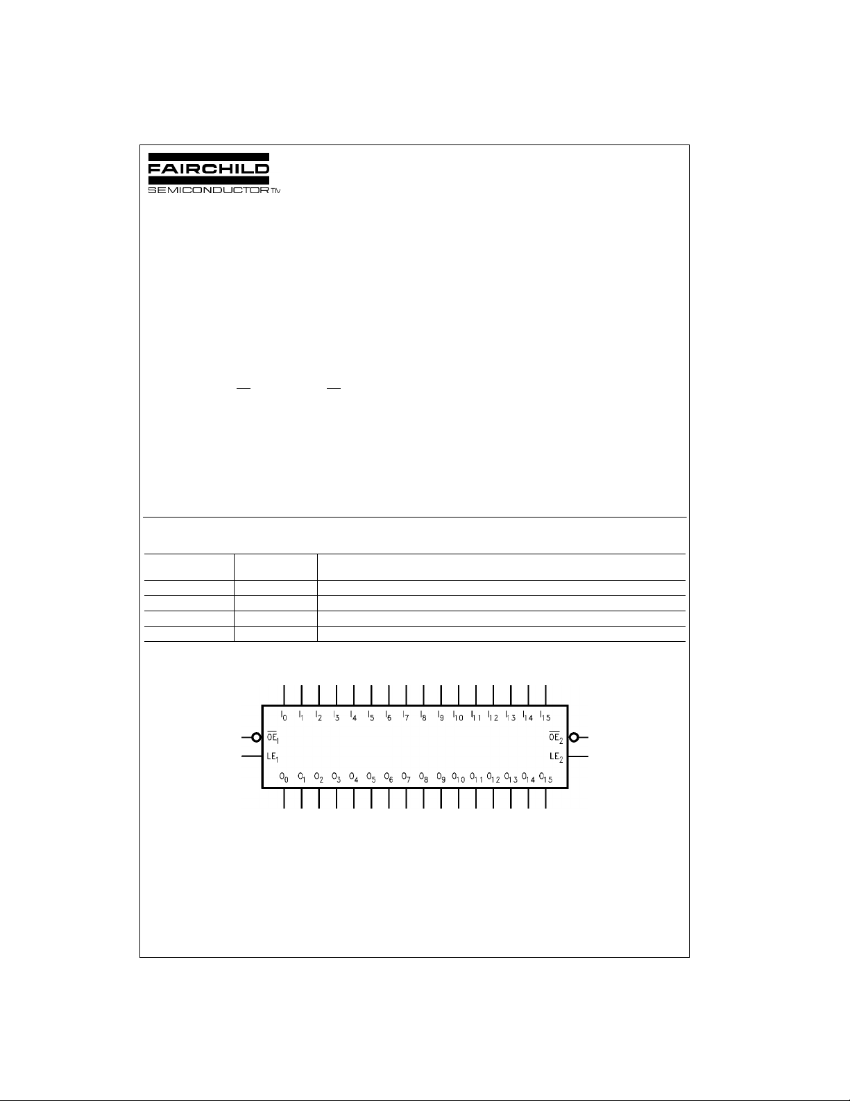
Logic Symbol
© 1999 Fairchild Semiconductor Corporation DS012021.prf www.fairchildsemi.com

Connection Diagram Pin Descriptions
Pin Names Description
OE
n
LE
n
I
0–I15
O
0–O15
Truth Tables
LE
74LVT16373 • 74LVTH16373
1
X H X Z
H L L L
H L H H
L L X O
LE
2
X H X Z
H L L L
H L H H
L L X O
H = HIGH Voltage Level
L = LOW Voltage Level
X = Immaterial
Z = HIGH Impedance
= Previous output prior to HIGH to LOW transition of LE
O
o
Output Enable Input (Active LOW)
Latch Enable Input
Inputs
3-STATE Outputs
Inputs Outputs
OE
1
I0–I
7
O0–O
o
Inputs Outputs
OE
2
I8–I
15
O8–O
o
7
15
Functional Description
The LVT16373 and LVTH16373 contain sixteen D-type la tches with 3-STATE standard outputs. The device is byte controlled with each byte functioning identically, but independent of the other. Control pins can be shorted together to obtain full
16-bit opera t i on . Th e f o l lo wi ng de s cri p t ion a pp l ie s to ea c h by te. W h en t he La t c h En a ble ( LE
enters the latches. In this condition the latches are transparent, i.e, a latch output will change states each time its D input
changes. When LE
HIGH-to-LOW transition of LE
is LOW, the latches store information that was present on the D inputs a setup time preceding the
n
. The 3-STATE standard outputs are controlled by the Output Enable (OEn) input. When OE
n
is LOW, the standard outputs are in the 2-state mode . When OEn is HIGH, the standard outputs are in the high impedance
mode but this does not interfere with entering new data into the latches.
www.fairchildsemi.com 2
) input is HIGH, data on the D
n
n
n

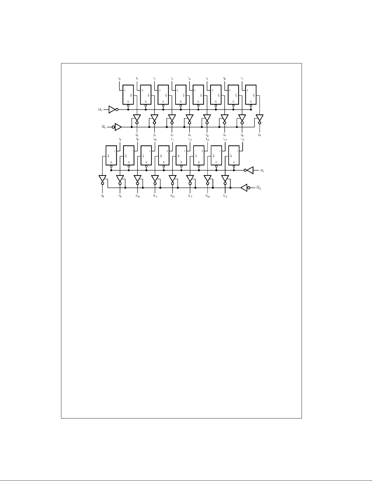
Logic Diagrams
Please note that thes e diagrams are provide d only for the understanding of logic operations a nd should not be used to est im ate propagation delays.
74LVT16373 • 74LVTH16373
3 www.fairchildsemi.com
 Loading...