Fairchild Semiconductor 74LVT162240MTDX, 74LVT162240MTD, 74LVT162240MEAX, 74LVT162240MEA Datasheet

© 1999 Fairchild Semiconductor Corporation DS012490 www.fairchildsemi.com
June 1999
Revised June 1999
74LVT162240 • 74LVTH162240 Low Voltage 16-Bit Inverting Buffer/Line Driver with 3-STATE Outputs and 25Ω
Series Resistors in the Outputs
74LVT162240 • 74LVTH162240
Low Voltage 16-Bit Inverting Buffer/Line Driver
with 3-STATE Outputs and
25Ω Series Resistors in the Outputs
General Description
The LVT162240 and LVTH162240 contain sixteen inverting
buffers with 3-STATE outputs designed to be employed as
a memory and address d rive r, clock driver, or bus oriented
transmitter/receiver. The device is nibble contr olled. Individual 3-STATE control inputs ca n be shorted toge ther for
8-bit or 16-bit operation.
The LVT162240 and LVTH162240 are designed with
equivalent 25Ω series resistance in both the HIGH and
LOW states of the output. This design reduces line noise in
applications such as memory address drivers, clo ck drivers, and bus transceivers/transmitters.
The LVTH162240 data inputs includ e bushold, eliminat ing
the need for external pull-up resistors to hold unused
inputs.
These inverting buffers and line drivers are designed for
low-voltage (3.3V) V
CC
applications, but with the capability
to provide a TTL interface to a 5V environment. The
LVT162240 and LVTH162240 are fabricated with an
advanced BiCMOS technology to achieve high speed operation similar to 5V ABT while maintaining a low power dissipation.
Features
■ Input and output interface capability to systems at
5V V
CC
■ Outputs include equivalen t series resistance of 25Ω to
make external termination resistors unnecessary and
reduce overshoot and undershoot
■ Bushold data inputs elimina te the nee d for exte rnal pul lup resistors to hold unused inputs (74LVTH162240),
also available without bushold feature (74LVT162240).
■ Live insertion/extraction per mitt ed
■ Power Up/Down high impedance provides glitch-free
bus loading
■ Functionally compatible with the 74 series 162240
■ Latch-up performance exceeds 500 mA
Ordering Code:
Device also available in Tape and Reel. Specify by appending s uffix let te r “X” to the ordering code.
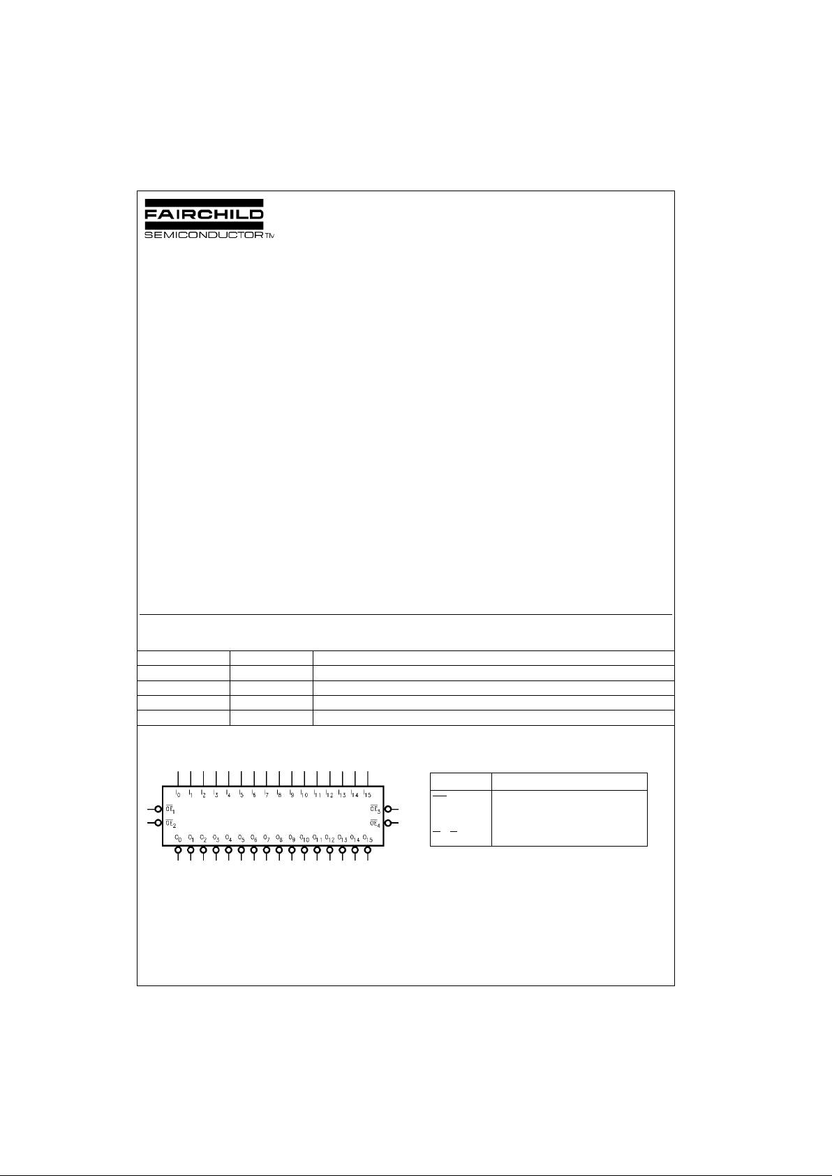
Logic Symbol Pin Descriptions
Order Number Package Number Package Description
74LVT162240MEA MS48A 48-Lead Small Shrink Outline Package (SSOP), JEDEC MO-118, 0.300” Wide
74LVT162240MTD MTD48 48-Lead Thin Shrink Small Outline Package (TSSOP), JEDEC MO-153, 6.1mm Wide
74LVTH162240MEA MS48A 48-Lead Small Shrink Outline Package (SSOP), JEDEC MO-118, 0.300” Wide
74LVTH162240MTD MTD48 48-Lead Thin Shrink Small Outline Package (TSSOP), JEDEC MO-153, 6.1mm Wide
Pin Names Description
OE
n
Output Enable Inputs (Active LOW)
I
0–I15
Inputs
O
0–O15
3-STATE Outputs

www.fairchildsemi.com 2
74LVT162240 • 74LVTH162240
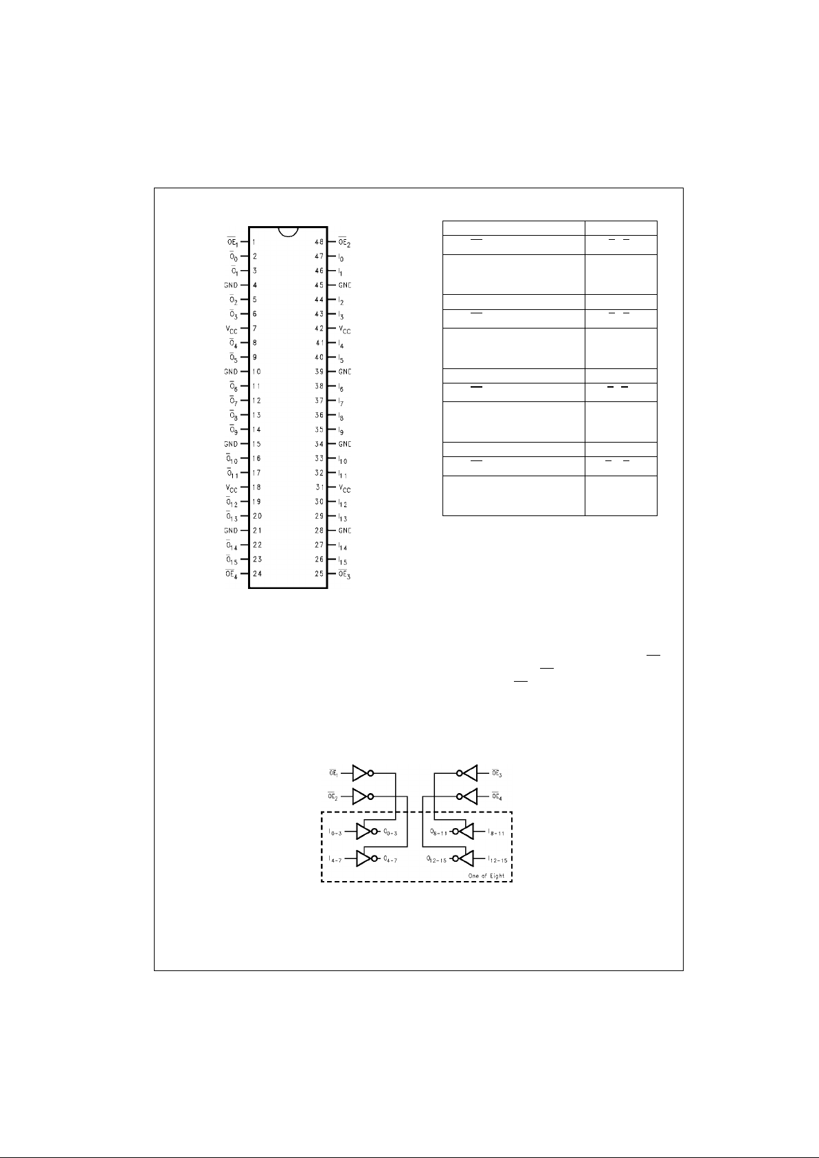
Connection Diagram Tr uth Table
H = HIGH Voltage Level L = LOW Voltage Level
X = Immaterial Z = High Impedance
Functional Description
The LVT162240 and LVTH162240 contain sixteen inverting
buffers with 3-STATE standard outputs. The de vice is nibble (4 bits) controlle d with each nibble functioning identically, but independent of the other. The control pins may be
shorted together to obtain full 16-bit operation. The 3-
STATE o utputs are controlled by an Output Enable (OEn)
input for each nibble. When OE
n
is LOW, the outputs are in
2-state mode. Wh en OE
n
is HIGH, the outputs are in the
high impedance mode, but this does not interfere with
entering new data into the inputs.
Logic Diagram
Please note that this diagram is provided o nly f or t he understanding of lo gic operations and should not be used to estimate propagation delays.
Inputs Outputs
OE
1
I0–I
3
O0–O
3
LLH
LHL
HXZ
Inputs Outputs
OE
2
I4–I
7
O4–O
7
LLH
LHL
HX Z
Inputs Outputs
OE
3
I8–I
11
O8–O
11
LLH
LHL
HXZ
Inputs Outputs
OE
4
I12–I
15
O12–O
15
LLH
LHL
HXZ
 Loading...