Fairchild Semiconductor 74LVQ373SJX, 74LVQ373SJ, 74LVQ373SCX, 74LVQ373SC, 74LVQ373QSCX Datasheet
...
74LVQ373
Low Voltage Octal Transparent Latch with 3-STATE
Outputs
General Description
The LVQ373 consists of eight latches with 3-STATE outputs
for bus organized system applications. The latches appear
transparent to the data when Latch Enable (LE) is HIGH.
When LE is low, the data satisfying the input timing requirements is latched. Data appears on the bus when the Output
Enable (OE) isLOW. When OE is HIGH, the bus output is in
the high impedance state.
Features
n Ideal for low power/low noise 3.3V applications
n Implements patented EMI reduction circuitry
n Available in SOIC JEDEC, SOIC EIAJ and QSOP
packages
n Guaranteed simultaneous switching noise level and
dynamic threshold performance
n Improved latch-up immunity
n Guaranteed incident wave switching into 75Ω
n 4 kV minimum ESD immunity
Ordering Code:
Order Number Package Number Package Description
74LVQ373SC M20B 20-Lead (0.300" Wide) Molded Small Outline Package, SOIC JEDEC
74LVQ373SJ M20D 20-Lead Molded Shrink Small Outline Package, SOIC EIAJ
74LVQ373QSC MQA20 20-Lead (0.150" Wide) Molded Shrink Small Outline Package, SSOP JEDEC
Devices also available in Tape and Reel. Specify by appending suffix letter “X” to the ordering code.
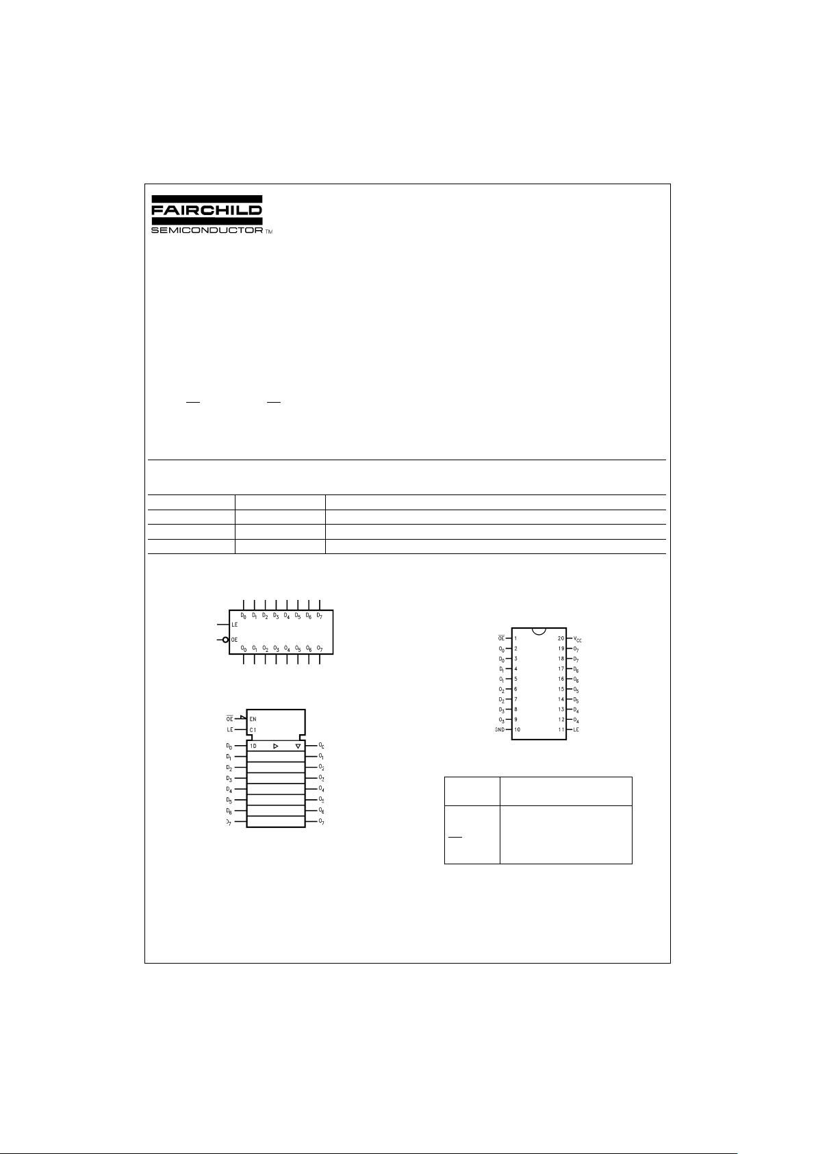
Logic Symbol Connection Diagram
Pin Descriptions
Pin
Names
Description
D
0–D7
Data Inputs
LE Latch Enable Input
OE
Output Enable Input
O
0–O7
3-STATE Latch Outputs
DS011359-1
IEEE/IEC
DS011359-2
Pin Assignment for
SOIC and QSOP
DS011359-3
May 1998
74LVQ373 Low Voltage Octal Transparent Latch with 3-STATE Outputs
© 1998 Fairchild Semiconductor Corporation DS011359 www.fairchildsemi.com

Functional Description
The LVQ373 contains eight D-type latches with 3-STATE
standard outputs. When the Latch Enable (LE) input is
HIGH, data on the D
n
inputs enters the latches. In this condition the latches are transparent, i.e., a latch output will
change state each time its D-type input changes. When LE is
LOW, the latches store the information that was present on
the D-type inputs a setup time preceding the HIGH-to-LOW
transition of LE. The 3-STATE standard outputs are controlled by the Output Enable (OE) input. When OE is LOW,
the standard outputs are in the 2-state mode. When OE is
HIGH, the standard outputs are in the high impedance mode
but this does not interfere with entering new data into the
latches.
Truth Table
Inputs Outputs
LE OE
D
n
O
n
XHX Z
HLL L
HLH H
LLX O
0
H
=
HIGH Voltage Level
L=LOW Voltage Level
Z=High Impedance
X=Immaterial
O
0
=
Previous O
0
before HIGH to Low transition of Latch Enable
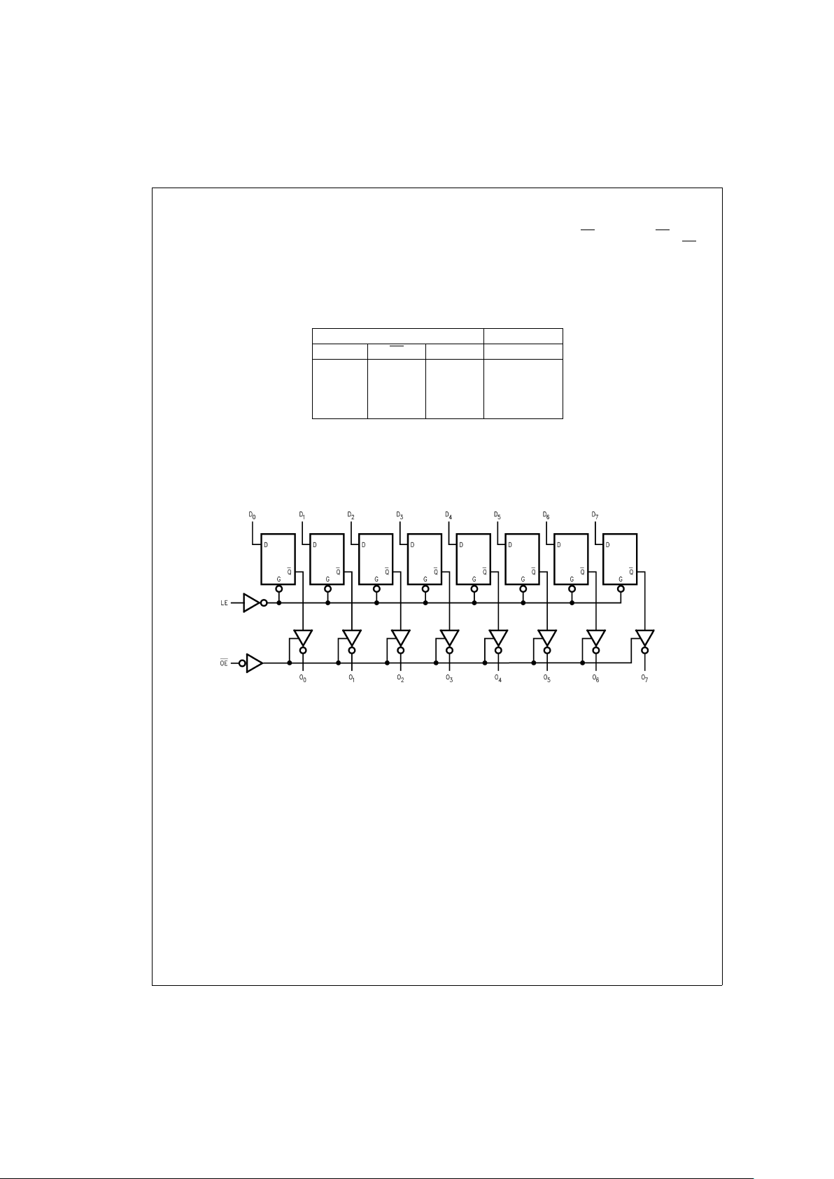
Logic Diagram
DS011359-5
Please note that this diagram is provided only for the understanding of logic operations and should not be used to estimate propagation delays.
www.fairchildsemi.com 2
 Loading...